Tensor Strain Measurement Using Advanced STEM
PRECISION STRAIN MEASUREMENT WITH TESCAN TENSOR FOR MATERIAL RESEARCH
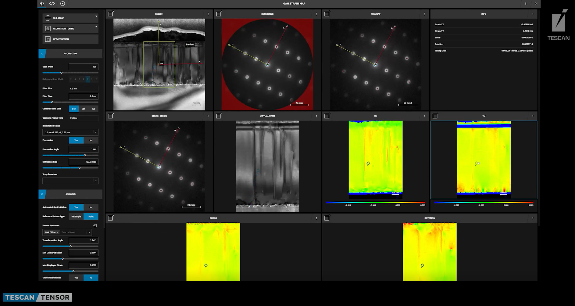
Strain measurement is one of the key capabilities of TESCAN TENSOR, a scanning transmission electron microscope (STEM) designed for advanced materials characterization. Utilizing the 4D-STEM technique enhanced by beam precession, enables the visualization and quantification of internal tension, compression and deformation of materials at the nanoscale. The seamless integration of full automation for alignments and on-the-fly data processing makes strain measurements accessible to a wide range of scientists and EM operators.
Explore the capabilities of TESCAN TENSOR
Watch the video below to see TESCAN TENSOR's strain measurement workflow in action.
Key Features:
-
Precession Electron Diffraction: Improves the quality of diffraction patterns for better data processing.
-
High Spatial Resolution: Measures strain in samples down to nanometer resolution.
-
High Precision and Accuracy: Determines strain values with a precision of about 0.05%.
-
Versatility: Suitable for a wide range of samples and materials in semiconductors and materials science.
-
Accessibility: Streamlined workflow for efficient and accurate data acquisition and analysis by any user.
Applications:
-
Semiconductor Industry: Characterizing strain in devices like transistors.
-
Materials Science: Studying defects and dislocations in materials.
-
Energy Storage: Analyzing strain in battery electrodes.
-
Aerospace: Investigating strain in structural components.
Benefits:
-
Enhanced Device Performance: Optimize devices by understanding strain-related effects.
-
Accelerated Research: Efficiently analyze and characterize materials.
-
Improved Product Quality: Ensure the reliability and durability of products.
Do you have any questions or need more information? Our experts are ready to assist you.
Thank you for Your interest.
Further reading