STEM Bright Field, Annular Dark Field and High-angle Annular Dark Field Imaging
Used primarily for sample navigation and feature size measurement, STEM images up to 1 gigapixel can be acquired quickly (up to 10 Mpixels/sec) with integrated, scintillator-based bright field and annular dark field / high-angle annular dark field detectors.
STEM Lattice Imaging
Optimized with automatically assisted alignment, you can use the STEM Lattice Imaging measurement to acquire atomic-resolution bright field (down to 2.8Å) and high-angle annular dark field (down to 3.5Å) STEM images.
Composition
Acquires elemental maps at high EDS count rates (>> 100 kcps), thanks to two symmetrically arranged, windowless EDS detectors, with a cumulative 2 steradian solid collection angle. Qualitative and quantitative EDS analysis is fully integrated in the user experience.
Orientation and Phase Mapping
Select the Orientation/Phase measurement for near real-time orientation, and phase mapping of single- and multi-phase polycrystalline and amorphous materials. A small electron beam (down to 1 nm) is scanned across the specimen while diffraction patterns are acquired at thousands of frames per second and are automatically indexed on the fly. Electron beam precession can be enabled with the push of a button to dramatically improve the quality of the results.
Strain Mapping
The Strain measurement combines nanobeam electron diffraction with electron beam precession to allow high-precision strain mapping in single crystals. Once a grain is tilted to a zone axis with the automation-assisted specimen tilting, a small (down to 1 nm) precessed electron beam scans across the crystal and acquires thousands of diffraction patterns. Precession improves the quality of the diffraction patterns for strain analysis by exposing more diffraction spots and producing more uniform spots. Strain maps are analyzed on-the-fly, to yield near real-time strain information to the operator.
Virtual STEM and Data Export
Virtual STEM is a highly configurable 4D-STEM measurement, that allows real-time reconstruction and visualization of STEM images from 4D-STEM datasets. Virtual spot or annular apertures can be defined by the user directly on acquired diffraction patterns, and images are reconstructed using those apertures. Alternatively, the analytical 4D-STEM dataset can be exported to open source, pixelated STEM data analysis and processing platforms, such as HyperSpy, LiberTEM or Py4DSTEM.
STEM Tomography
The STEM Tomography measurement provides assisted and automated acquisition of specimen tilt series using STEM imaging signals (BF, DF and HAADF) and reconstruction of those tilt series into 3D volume datasets. Acquired data can be exported for advanced reconstruction, analysis and visualization in a range of 3D imaging software, including TESCAN's 3D Volume Analysis software.
EDS Tomography
The EDS Tomography measurement provides assisted and automated acquisition of specimen tilt series using STEM and EDS signals and reconstruction of those tilt series into 3D elemental maps. Acquired data can be exported for advanced reconstruction, analysis and visualization in a range of 3D imaging software, including TESCAN's 3D Volume Analysis software.
Diffraction Tomography
TESCAN TENSOR can also be used for 3DED (micro-ED) diffraction tomography acquisition and analysis. A nearly parallel nanobeam, with or without precession, can be focused in a spot as small as 20 nm, and diffraction patterns are acquired while the specimen is tilted through a large range of angles, providing a superior solution for the structural analysis of synthetic or natural sub-micron and nanoparticles. The optional PETS Advanced software can be used to analyze the 3D Precession Electron Diffraction (3DPED) dataset to yield the unit cell dimensions.
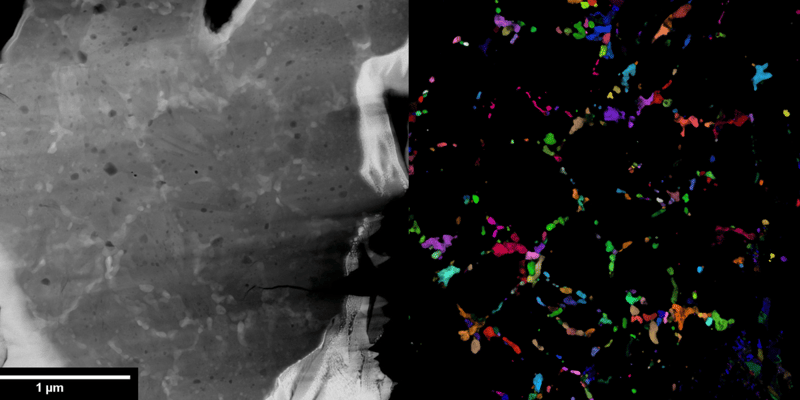
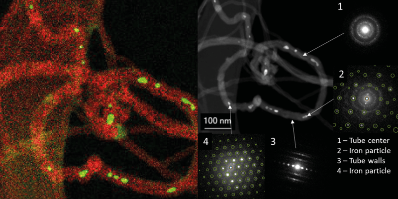
Multimodal Chemical and Crystallographic Characterization of Carbon Nanotube encapsulated Metal Particles
Precise identification of both structure and chemistry on the nanoscale can be leveraged to advance research into the next generation of engineering materials, across industry and academia. This TESCAN TENSOR application note provides an example of multimodal chemical and crystallographic characterisation of metal particles encapsulated within carbon nanotubes.
By combining STEM imaging, nanobeam diffraction with crystal orientation analysis (4D-STEM) and EDX mapping, we can work towards a comprehensive understanding of this material system. This application note was produced in collaboration with Prof. Andy Brown and Dr. Zabeada Aslam of Leeds University (UK).

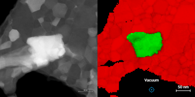
Phase and Orientation Analysis of Bismuth Germanium Oxide (BGO) on Evaporated Aluminum
TESCAN TENSOR provides 4D STEM capabilities enabling fast nanoscale phase and orientation analysis. In this technical note, the methodology of phase and orientation analysis is described, subjected to dropcasted BGO (Bi12GeO20) on evaporated aluminum. BGO has a relatively large lattice parameter of 10.1Å, and Al a much smaller lattice parameter of 4.1Å, revealing clearly differentiated electron diffraction patterns due to this large difference in lattice parameter.
Phase and Orientation of BGO is measured from a scanning diffraction dataset, by matching the acquired electron diffraction patterns with BGO and Al templates, for each pixel in the dataset. It is shown how precession electron diffraction (PED) improves the confidence of indexing, by enhancing the number of reflections in the diffraction pattern, leading to greater differentiation of the information contained in the patterns acquired from the two phases.

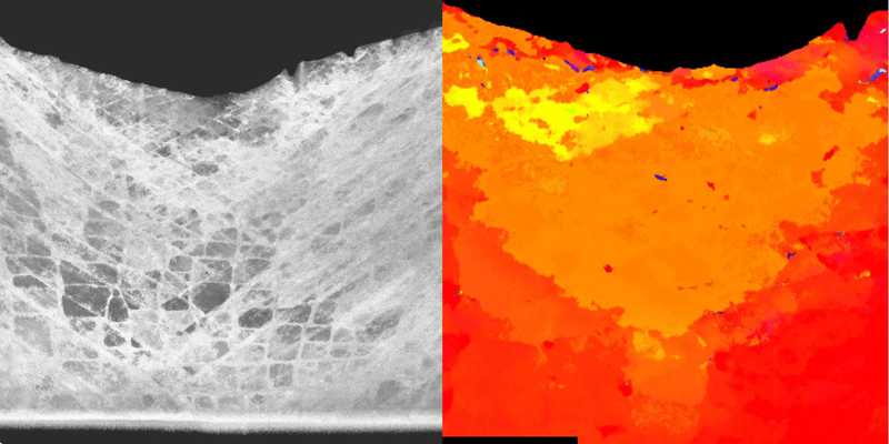
Deformation behavior in Ni-based superalloys revealed by 4D-STEM crystal orientation analysis
This application note presents a study into Vickers indentation induced plastic deformation in Nickel superalloys. Precession assisted 4D-STEM with automated crystal orientation analysis was used to investigate deformation induced, nanoscale grain re-orientation, in a site-specific FIB prepared specimen.
Fast acquisitions, and on-the fly-processing enabled measurements to be optimized, and specimen areas to be localized, in a near real-time iterative manner, which vastly increases measurement and microscope time efficiency. This application note was prepared in collaboration with Sicong Lin and Prof. Kai Chen from State Key Laboratory for Mechanical Behavior of Materials, Xi'an Jiaotong University, China, as well as Penghan Lu and Prof. Rafal E. Dunin-Borkowski at the Ernst Ruska-Centre for Microscopy and Spectroscopy with Electrons FZ Jülich, Germany.

4D-STEM phase and orientation analysis of lithium-ion battery anode materials
The differentiation of lithium phosphates in battery anodes is a challenging task due to the relatively similar elemental compositions of the different phosphate phases. In this application note we show how TESCAN TENSOR’s 4D-STEM phase analysis, using precession electron diffraction patterns, helps to improve the differentiation of these phases. The distribution and relative orientation relationship between different phases in the battery anode can be easily deduced using this analysis.
We also show how titanium oxide particles are preferentially distributed along phosphate particle grain boundaries. This application note is prepared with Dr. Roland Schierholz and Prof. Rüdiger-A. Eichel at the Institute for Energy and Climate Research, FZ Jülich, Germany, as well as Penghan Lu and Prof. Rafal E. Dunin-Borkowski at the Ernst Ruska-Centre for Microscopy and Spectroscopy with Electrons, FZ Jülich, Germany.