Key Benefits of TESCAN Rocking Stage
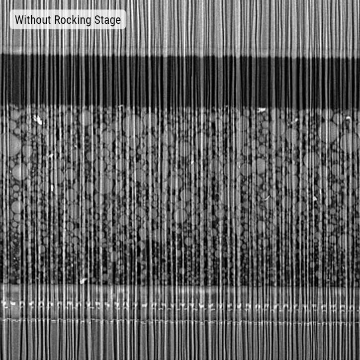
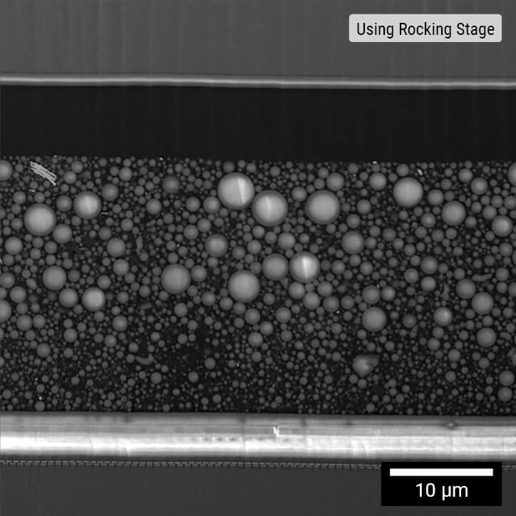
Fixed angle polishing vs rocking polishing. Rocking polishing delivers effective removal of curtaining artefacts.
Curtaining Artifacts Being Gone

Eliminate FIB-induced curtaining artifacts caused by preferential milling rates, surface topography, or internal sample geometry for improved imaging results.
Precision at Your Fingertips

Achieve accurate end-pointing at your region of interest with SEM live monitoring throughout the milling and tilting process.
Boost Your Sample Preparation Efficiency

Maximize throughput with the TESCAN Rocking Stage set-up wizard, automating rocking procedures and positions.
Adapt to Complex Samples

Enhance final sample quality for failure analysis of semiconductor devices or advanced materials with artifact-free FIB cross-sectioning and cross-section polishing.
Versatility Meets Compatibility

Benefit from the new design featuring full compatibility with load locks, Beam Deceleration Mode (BDM), and the RSTEM detector, without sacrificing system versatility.

Advanced Applications for TESCAN Rocking Stage
Master the Art of Failure
Analysis
Improve the final sample quality in failure analysis of semiconductor devices or advanced materials by leveraging the TESCAN Rocking Stage's artifact-free FIB cross-sectioning capabilities.
Perfect Your
Tomography
Enhance FIB-SEM tomography acquisition by minimizing curtaining artifacts and achieving pristine imaging results with the TESCAN Rocking Stage.
Handle Large and Flat Samples with Ease
Manage an extensive array of samples and facilitates your study of a diverse sample range with the versatile design of TESCAN Rocking Stage.