
TESCAN AMBER X 2 for Delayering
Uniform
Delayering

Achieve consistent, artifact-free delayering by leveraging our tailored Nanoflat Chase and C-maze gas chemistries optimized for sub-10 nm technology nodes.
Device
Integrity

Preserve electrical properties with our precise, low kV Plasma FIB milling, employing inert Xe ions for delicate sample processing.
Failure
Localization
Streamline defect isolation with our refined in-lens detection, engineered for effective passive voltage contrast imaging.
Delayering
Automation
Simplify end-point determination with our intelligent TESCAN DelayeringTM software, automating delayering to the targeted layer.
Electrical
Analysis
Facilitate in-situ verification or characterization of electrical failures using compatible industry-leading nanoprobing solutions.
User
Productivity

Boost operational efficiency for users at all expertise levels with the intuitive TESCAN EssenceTM graphical user interface.
Discover TESCAN AMBER X 2
for Delayering


The Advantages of TESCAN AMBER X 2 for Delayering
Utilize SEM-Based Nanoprobing for detailed characterization of NMOS and PMOS transistors across various semiconductor nodes, facilitating precise layer targeting for effective delayering.
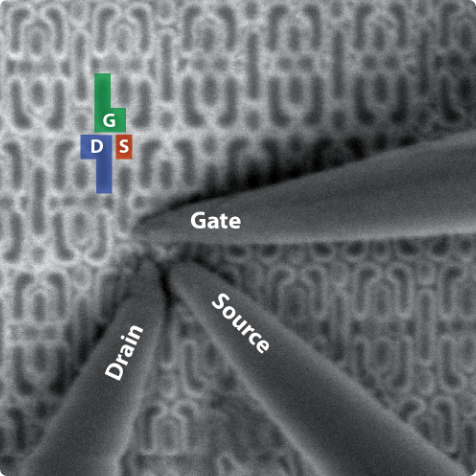
In-depth SEM-based Nanoprobing
Leverage sophisticated SEM-based
Nanoprobing to accurately
characterize NMOS and PMOS
transistors across a spectrum of
semiconductor nodes, including
22, 14, 10, and 5 nm.
Targeted Uniform Delayering
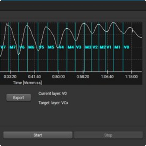
Attain meticulous uniform delayering, empowered by advanced automation that intelligently identifies and halts at your designated layers within the stack.
Consistent Large-Area Delayering
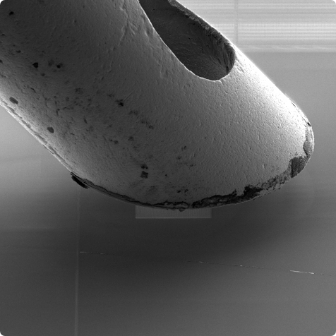
Ensure expansive, uniform delayering over large areas measuring 300 × 300 μm2, utilizing our specialized "drilled" nozzle.