
Comprehensive
Delayering
Execute thorough plasma FIB delayering across thicker intermediate and I/O device layers, securing superior process control beyond traditional methods.
Layer Stack
Mastery
Navigate through the entire layer stack with precision, or tailor delayering for older technologies, utilizing combined methodologies in a single plasma FIB system.
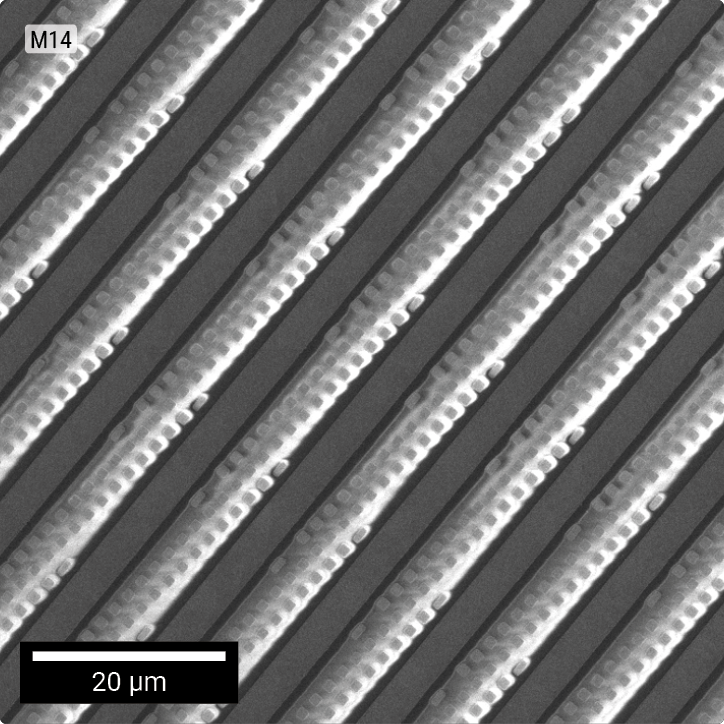
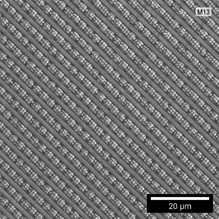
Images show uniform delayering through M14 and M13 metal/via layers of the device.
Monitoring
Excellence
Meticulously observe the delayering process with peak recognition in the EPD curve, facilitated by continuous In-Beam BSE signal assessment.
Planarity
Assurance
Attain optimal delayering planarity by employing a specialized clamp holder, ensuring sample horizontality superior to conventional mounting techniques.
Recipe
Customization
Develop tailored delayering protocols specific to your lab's requirements, with stored settings that expedite transitions between sample types.
Confident
Deprocessing
Rely on validated software guidance from our partners for defining and monitoring multi-position milling, ensuring thorough and precise layer removal.
Advanced Capabilities with TESCAN Low Angle Polishing
Discover the benefits of TESCAN EssenceTM for enhanced sample alignment, consistent delayering, and accurate monitoring, all contributing significantly to the depth and precision of your research.
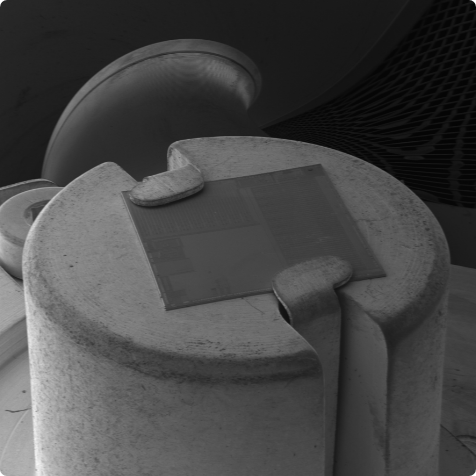
Dedicated clamp sample holder to ensure better horizontality of the sample for deprocessing
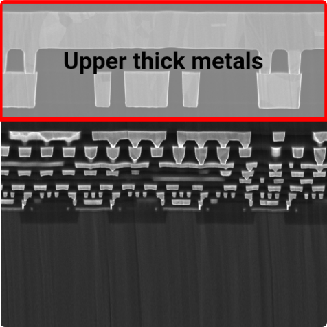
Homogeneous plasma FIB delayering of thicker intermediate layers or Input-Output (I/O) areas of semiconductor devices
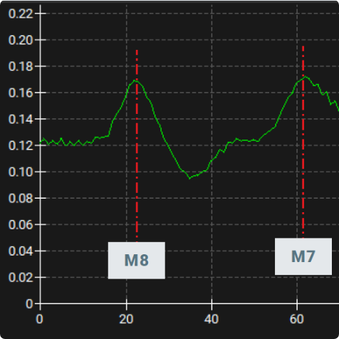
Live monitoring of the intensity profile based on the in-column BSE signal plotted into the live monitor graph in TESCAN EssenceTM Low Angle Polishing module.