
Efficient Resource Utilization

Empower your research with a system that utilizes pre-programmed recipes for unattended, consistent Plasma FIB delayering, preserving device integrity.
Proprietary Chemistry Integration
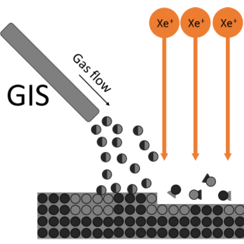
Benefit from the synergy of Xe Plasma FIB with TESCAN's gas chemistry crafted for optimal delayering across contemporary semiconductor nodes.
.png?width=734&height=617&name=image1_higher%20kopie%20(1).png)
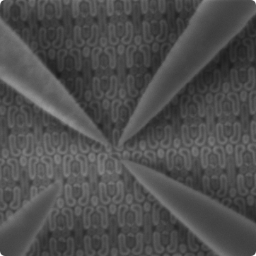
Automated delayering through several bottom layers of 7 nm FinFET CPU device using Nanoflat and C-maze chemistry.
Customization and
Consistency

Craft and apply unique delayering processes with predefined templates, ensuring uniform application and repeatability across samples.
In-depth
Monitoring
Track delayering progress with sophisticated end-point detection, leveraging peak recognition within the TESCAN Delayering module for precision halting.
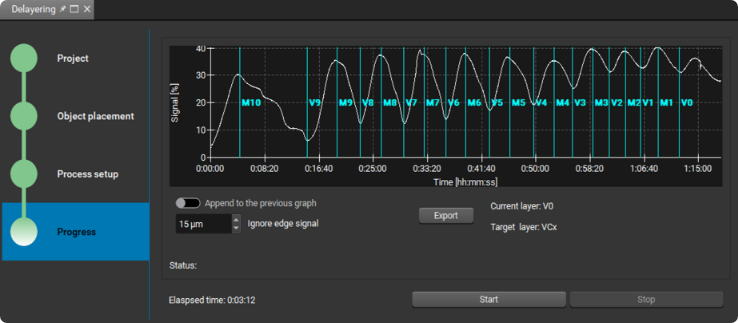

A) Live peak detection on FIB end-point signal during delayering process.
B) 14 nm device delayered to M0. Imaging and probing at 500 eV.
Uninterrupted
Assurance
Rely on automated processes designed to terminate delayering before reaching critical layers, safeguarding device functionality.
Advanced Applications for EssenceTM Automated Delayering
Enhanced Imaging
Utilize sub-1 kV SEM imaging for distinct voltage contrast and swift failure identification.

Chemistry Options
Choose from diverse delayering chemistries like Nanoflat, Chase, and C-maze, tailored for various sample types.
EssenceTM Module
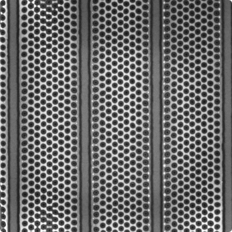
Leverage the Essence Delayering module for uniform etching across the 3D NAND stack, ensuring thorough analysis.