WHY NANOSCALE CHARACTERIZATION MATTERS IN SEMICONDUCTORS
What if you could see how the grain structure of your key layers varies with annealing?
Or with different processing conditions?
And how do grain structure and orientation correlate to compositional variation and segregation?
Wouldn’t it be a game changer if you could see all of this on the same sample?
Technology development and production of new materials and semiconductor devices requires morphological, structural, and chemical characterization at the nanoscale level to understand their chemical-physical properties and to optimize their production process.
The electrical performance of semiconductor devices depends strongly on the type and distribution of crystalline phases in the individual layers, which can be affected during the deposition process or individual annealing steps.
For semiconductor manufacturers, these analyses are critical for failure analysis, yield debugging, and process development.
The dream of microscopy has been the ability to see all of these in the actual sample, in their true geometry instead of on test coupons or proxy samples, or from assimilating data from multiple samples.
Advanced Methods of 4D-STEM Electron Microscopy
With the TESCAN TENSOR, now you can get all of this insight on the same sample with astonishing ease of measurement.
The advanced methods of 4D-STEM electron microscopy extend the capabilities of the traditional (S)TEM imaging and EDS compositional analysis techniques by providing structural information at each pixel of an acquired STEM image.
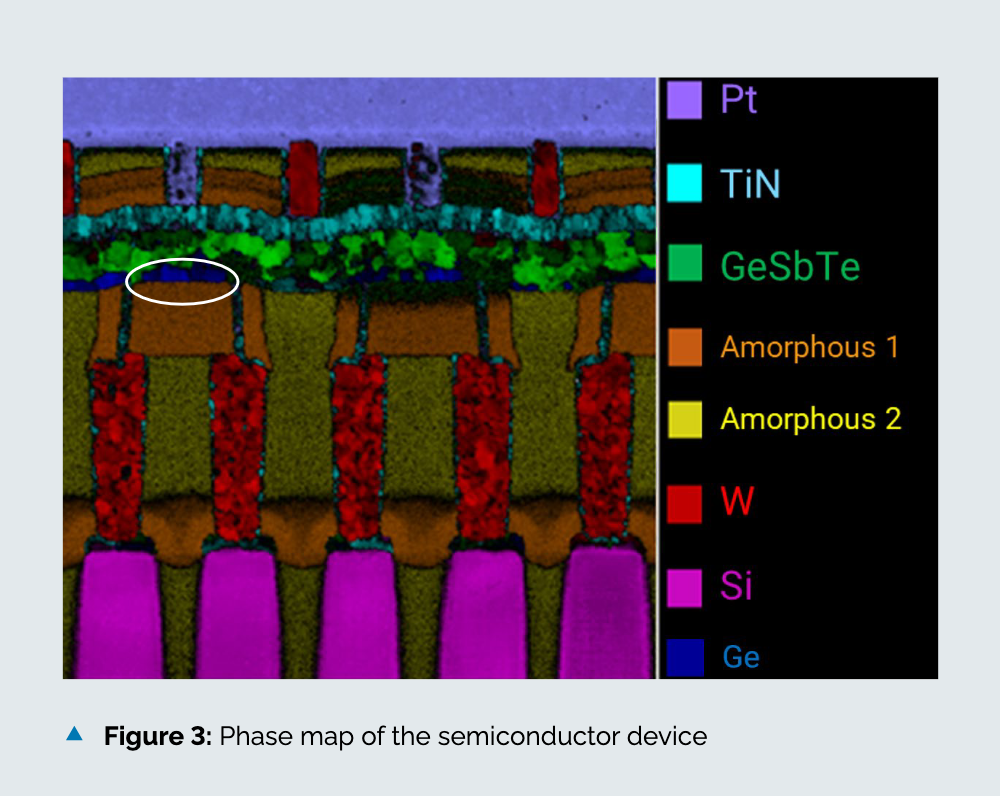
In this application note, we show how a 4D-STEM phase mapping experiment revealed the separation of germanium from the GST layer at the interface with two distinct amorphous phases, while simultaneously gathering imaging and EDS maps of the same device.
Using the TESCAN TENSOR, the new state-of-the-art analytical STEM tool, results like those in this application note can be achieved by any user regardless of their expertise in electron microscope optics and imaging modes. TENSOR seamlessly integrates beam precession with beam blanking and readout of 4D-STEM data using a very fast and sensitive direct electron detector to maximize the quality and accuracy of acquired data. High levels of automation then enable operators to focus on sample analysis instead of aligning and tuning the microscope. Moreover, multimodal acquisition and analysis of 4D-STEM and EDS data further improves the quality and accuracy of phase mapping experiments.