TESCAN Launches SOLARIS 2, SOLARIS X 2, and AMBER X 2 for Semiconductor Analysis

New systems enhance semiconductor research with automated TEM lamella preparation, advanced failure analysis, and precision delayering with in-situ electrical analysis.

Brno, Czech Republic, (DATE) – TESCAN GROUP, a global leader in scientific instrumentation, announces the launch of three advanced systems: SOLARIS 2, SOLARIS X 2, and AMBER X 2. These solutions are developed to meet the increasing demands of semiconductor failure analysis, offering automation, precision, and efficiency for sub-10 nm technology nodes and beyond. 

To provide further insights into these new systems, TESCAN will be hosting a webinar on (DATE). From October 28 to November 1, TESCAN experts will also be available at ISTFA 2024 in San Diego, California, to discuss these innovations and their applications in semiconductor analysis. 


TESCAN SOLARIS 2: AI-Driven TEM Lamella Preparation 


The TESCAN SOLARIS 2 is designed for fully automated TEM lamella preparation using the AI-powered TESCAN TEM AutoPrep™ Pro software. This system produces high-quality, ultra-thin samples for sub-10 nm technology nodes, such as advanced logic and memory devices. 


Key features include: 


  • Fully Automated TEM Lamella Preparation: AI-driven precision delivers high-quality samples with minimal damage, supporting various geometries such as top-down, planar, and inverted lamellae. 
     
  • Flexible Sample Handling: Achieve high-resolution end-pointing for advanced devices like GAA and FinFET transistors with the Triglav™ SEM column. 
     
  • User-Friendly Operation: Automated workflows reduce setup time and optimize system readiness, ensuring productivity for users at all experience levels. 


TESCAN SOLARIS X 2: Ga-Free TEM Preparation and Advanced Failure Analysis 


The TESCAN SOLARIS X 2 extends the capabilities of physical failure analysis with its Mistral™ Xe Plasma FIB column, providing large-area cross-sectioning and gallium-free TEM lamella preparation for complex semiconductor packages, including 2.5D, 3D IC, and MEMS devices. 


Key features include: 


  • Large-Scale Failure Analysis: Perform deep cross-sectioning, reaching buried structures up to 1 mm in depth, using the Mistral™ Xe Plasma FIB. 
     
  • Ga-Free TEM Lamella Preparation: Produce high-quality, gallium-free lamellae, preserving sample integrity for advanced packaging applications. 
     
  • Precise Defect Targeting: The Triglav™ SEM column enables nanometer-level accuracy for defect isolation in advanced semiconductor packaging. 


TESCAN AMBER X 2: Precision Delayering with In-Situ Electrical Analysis 


The TESCAN AMBER X 2 provides precision delayering with uniform, artifact-free results, supporting sub-10 nm technology nodes. This system is built for electrical failure analysis, allowing in-situ verification through SEM-based nanoprobing and efficient defect isolation. 


Key features include: 


  • Uniform, Artifact-Free Delayering: Achieve consistent results with tailored gas chemistries like Nanoflat Chase and C-maze, optimized for NMOS and PMOS transistors. 
     
  • In-Situ Electrical Analysis: SEM-based nanoprobing allows real-time characterization of electrical failures during the delayering process. 
     
  • Automated Delayering: TESCAN Delayering™ Software automates end-point determination, targeting specific layers for detailed failure analysis. 


These systems are built to address the growing complexities of modern semiconductor technologies, improving the efficiency and accuracy of failure analysis for researchers and engineers. 


Join Our Webinar 


TESCAN is hosting an exclusive webinar, “Introduction to TESCAN’s FIB-SEM Solutions for Semiconductor Failure Analysis and R&D Laboratories,” which will offer an in-depth look into the capabilities of our platforms, including cross-sectioning, TEM preparation, and delayering. 


  • Date & Time: Mon, Oct 21, 2024 5:00 PM - 6:00 PM CEST 


Meet Us at ISTFA 2024 

TESCAN will also be present at ISTFA 2024 from October 28 to November 1, 2024, where our solutions can be experienced firsthand. Our experts will be available at booth #NUMBER to answer questions and provide insights into how our systems can enhance semiconductor failure analysis.

For more details, visit us at ISTFA or learn more on our website.

AI/ML-Enhanced Techniques: Improving Efficiency and Accuracy in Failure Analysis

FA 4.0 aims to transform the failure analysis field by developing advanced equipment and methods, utilizing the capabilities of artificial intelligence, machine learning, and automation. The project's main innovations include:

  • § Advanced devices and equipment for failure analysis
  • § Incorporation of AI/ML-driven algorithms for image and signal analysis to improve tool performance
  • § Simplifying complex workflows by interconnecting devices with novel hardware interfaces
  • § Centralizing diagnostic data collection and correlation for efficiency
  • § Detailed defect mode detection and cataloging, incorporating metrology and electrical test data

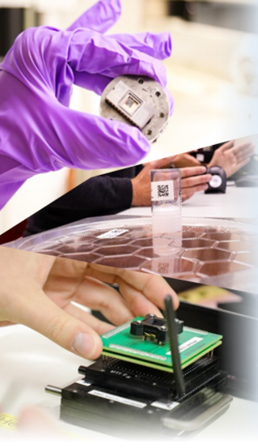
An international consortium from Germany, France, and the Czech Republic, including industry leaders such as Infineon, STMicroelectronics, and BOSCH, have collaborated with SMEs, medium-sized companies, and renowned research institutes to realize this project.

Enhancing Failure Analysis with AI/ML-Driven Solutions

FA 4.0 is focused on maximizing the potential of AI/ML solutions to transform failure analysis. By using standardized hardware and software, the project aims to integrate tools and FA databases, enabling streamlined workflows. This approach facilitates the development of advanced AI/ML solutions, improving FA quality and productivity, and enabling failure analysis engineers to work more efficiently.

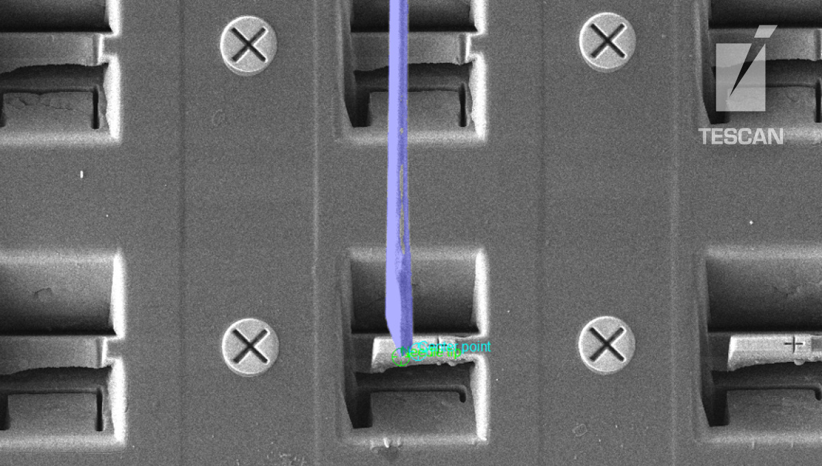
FA 4.0 is expanding current FA capabilities for measurement evaluation with signal and image-based AI/ML methodologies. These advanced techniques include AI/ML-driven evaluations of raw signals from detectors in SEMs and FIBs, as well as acoustic echoes in Scanning Acoustic Microscopes and X-Ray signals in micro CT. This enables the development of next-generation FA tools, promoting AI/ML-based, integrated workflows that enhance productivity and quality in the future of failure analysis.

Looking Towards the Future of Failure Analysis

By September 2023, TESCAN and project partners aim to implement a fully functional workflow comprising:

  • § Package defect localization/identification in PVA TEPLA's Scanning Acoustic Microscope
  • § Large volume material removal on the shared FA 4.0 stage using 3D-Micromac's laser micromachining tool,with data transfer via image header
  • § Fine sample preparation and defect analysis with SOLARIS X.

In conclusion, TESCAN and its FA 4.0 partners aim to pioneer a new phase of failure analysis, where AI/ML-driven solutions and automation enhance efficiency, accuracy, and reliability. We strive to shape the future of electronic systems and improve Europe's standing in the field of smart mobility and industrial production.

Join us as we continue this significant endeavor to redefine failure analysis!

fa-4-01-1

About TESCAN GROUP   

TESCAN was established in 1991 and has grown from a 4-5 engineer start-up initially, to a company with more than 700 employees working from more than 10 facilities in 8 countries. We are a leading player in charged-particle optical instrumentation, including Scanning and Scanning Transmission Electron Microscopy (SEM & STEM), Focused Ion Beam (FIB) and X-ray Computed Tomography (micro-CT), with more than 4000 instruments sold and operational in more than 80 countries.  


In 2013, it expanded by merging with ORSAY PHYSICS, a French global leader in customized focused ion and electron beam technologies, and in 2018 by acquiring XRE, a Belgian innovator in the field of Dynamic and micro-CT technologies. A further, more recent milestone was the acquisition in 2023 of TESCAN ORSAY HOLDING and all its subsidiaries by CARLYLE, a US private equity company. TESCAN GROUP is headquartered in Brno, Czech Republic, where most of our instruments are expertly assembled, tested, and shipped to customers across the globe.

Press Contact     

For further information, interview requests, or media inquiries, please contact:     

Linda Bilal, Senior Global Marketing Manager    


Marketing Department     

TESCAN GROUP, a.s.; Libušina tř. 21; 623 00 Brno – Kohoutovice; Czech Republic     

Phone: +420 530 353 478, Email: linda.bilal@tescan.com