Precision Without Compromise
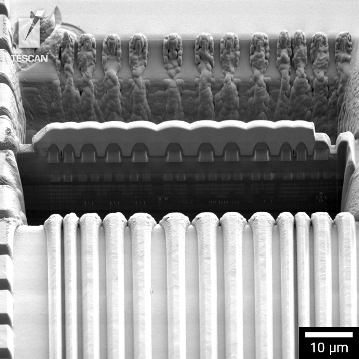
SOLARIS 2 delivers exceptional FIB resolution with minimal beam damage and milling artifacts. It’s not just for standard (top-down) lamella - you’ll also master inverted, planar, and double-cross lamella with our optimized single-step in-situ lift-out geometries, ensuring your samples are ready with precision and efficiency.
Ga FIB Meets UHR-SEM Immersion Optics
Experience the powerful combination of Ga-focused ion beam and ultra-high-resolution SEM immersion optics. This integration ensures top-tier performance in ion beam milling and SEM end-pointing, offering unmatched surface sensitivity and contrast, even on the most complex semiconductor samples.


Maximize Your TEM Sample Preparation with SOLARIS 2
Intelligent Automation

Automatically craft high-quality TEM samples with minimal damage, hands-free.
Advanced
Flexibility

Adapt to any lamella geometry with exceptional quality and reduced amorphization.
Precision
Targeting

Achieve unparalleled surface sensitivity and material contrast across diverse electronic devices and structures.
Consistent
Readiness

Get repeatable, high-quality results without lengthy alignments or setups.
Customizable Workflows

Seamlessly switch between semi-automated and fully automated sample prep tailored to your specific needs.
Intuitive
Operation

Obtain superior data quality with ease, regardless of your FIB-SEM expertise.

Discover how to prepare TEM samples
from logic, memory, and 3D NAND.
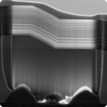
Main Benefits of TESCAN SOLARIS 2
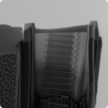
Fast, Precise TEM Samples
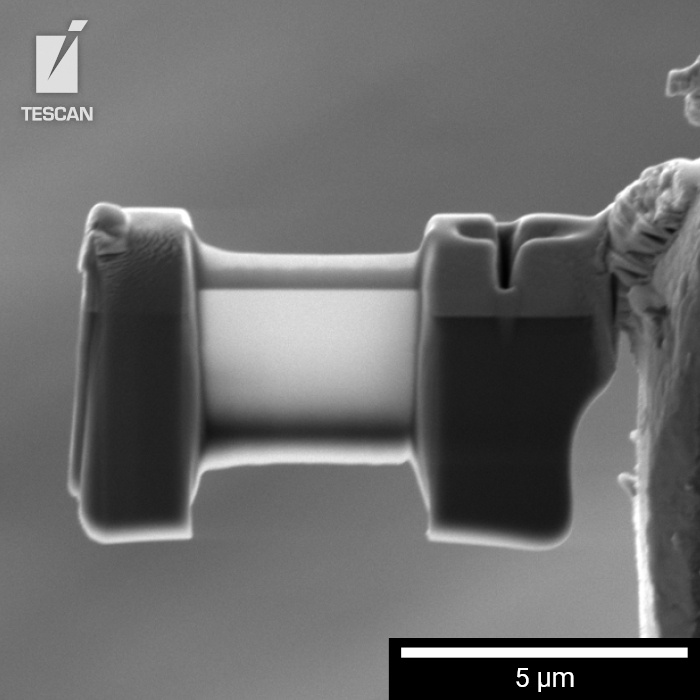
Produce ultra-thin TEM samples from sub-10 nm nodes in under an hour with TESCAN TEM AutoPrep™ Pro. Fully automated from lift-out to final FIB polishing, it delivers consistently superior results every time.
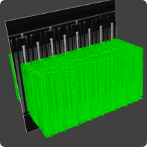
Pinpoint Accuracy for Advanced Devices
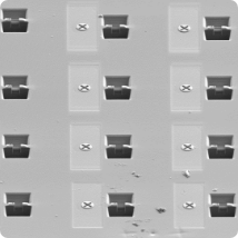
Target single transistor lines in GAA or FinFET devices with pinpoint accuracy using AI-driven fiducial mark recognition and high-resolution imaging from the Triglav™ SEM column featuring advanced SE and BSE detectors for enhanced contrast at the beam coincident point.
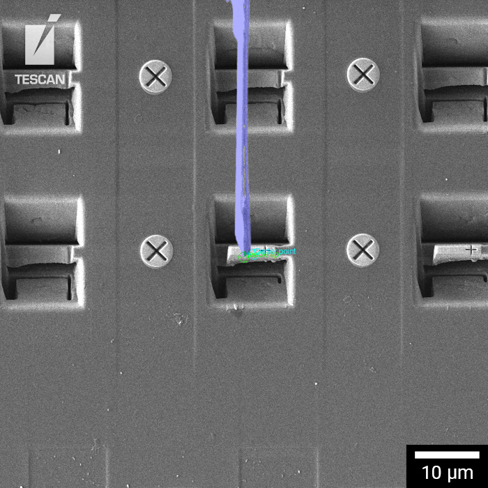
Adaptable Lamella Prep with OptiLift™
Prepare top-down, planar, and inverted lamella effortlessly with the OptiLift™ nanomanipulator, strategically placed “below FIB.” This innovative design eliminates the need for extra flipping devices, simplifying your workflow.
Always Ready, Always Aligned
Keep your system ready with automated electron and ion column alignments that run overnight, ensuring minimal setup and maximum uptime.
High-Resolution Imaging Excellence
The Triglav™ SEM column, designed for ultra-high-resolution imaging, delivers outstanding surface sensitivity and contrast, making it ideal for beam-sensitive materials.
Streamlined Productivity
The redesigned TESCAN TEM AutoPrep™ Pro offers intuitive navigation between processes and extensive customization for any TEM lamella workflow, boosting productivity for every user.