
Enhanced Sample Preparation Throughput
TESCAN SOLARIS X 2 extends FIB physical failure analysis capabilities to large-area applications, making deep cross-sectioning of advanced packaging devices, displays, MEMS, and optoelectronic devices more efficient.
Featuring the new generation Mistral™ Xe Plasma FIB column, SOLARIS X 2 offers increased maximum ion beam current and a sharper ion beam profile across the full range, with significantly reduced beam tails. This allows operators to use higher milling and polishing currents, achieving superior surface quality comparable to conventional Plasma FIB, but with greater speed and precision.

SOLARIS X 2: Expanding Plasma FIB-SEM Capabilities for Large and Small-Scale Applications
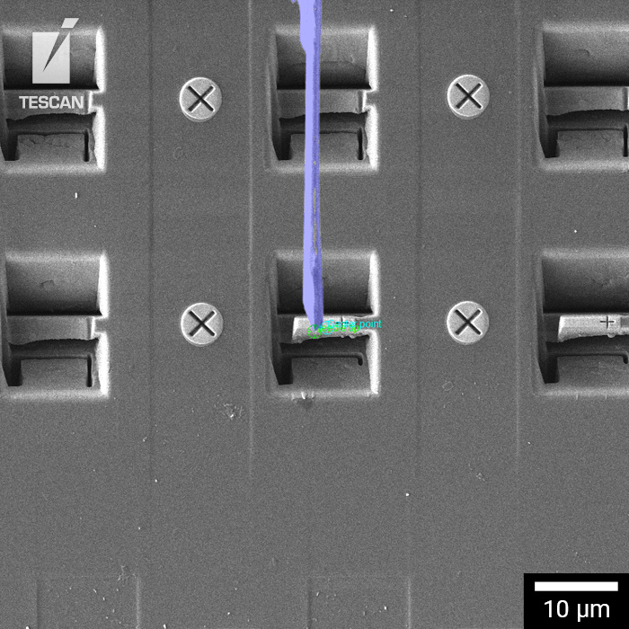
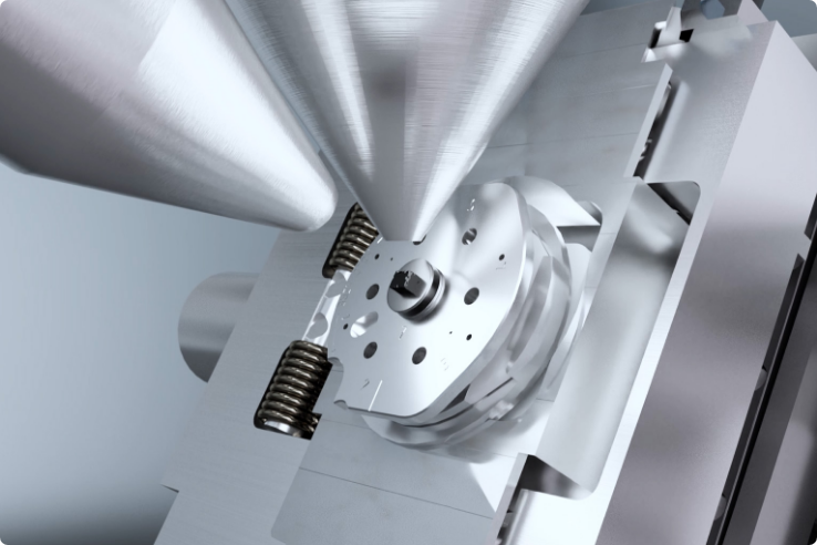
As TESCAN’s flagship Plasma FIB-SEM microscope, SOLARIS X 2 is designed to deliver ultimate resolution and signal strength at the FIB and SEM beams coincidence point. This precision enables operators to accurately end-point on the smallest defects within complex IC package stacks, HBM memories, and other heterogeneously integrated devices.
Enhanced ion beam properties reduce typical FIB artifacts, minimizing the need for alternative high current polishing methods, and enabling automated TEM lamella preparation and efficient sub-100 µm cross-sectioning.


How TESCAN SOLARIS X 2 Fits Your Needs
Purpose-Driven Performance

Accelerate physical failure analysis with the fast material removal capabilities of the Xe Plasma FIB beam.
Deep Sample
Access

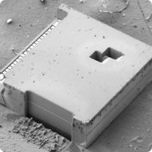
Reach buried structures up to 1 mm in depth using ion beam currents up to 3.3 μA.
Precision
at the Nanoscale

Achieve precise end-pointing with nanometer accuracy during milling or cross-sectioning, thanks to the high-resolution imaging of the Triglav™ SEM column.
Superior Surface Sensitivity

Conduct ultra-high-resolution imaging on beam-sensitive materials with the Triglav™ SEM column, designed for excellent surface sensitivity and contrast.
Pristine Sample Preservation

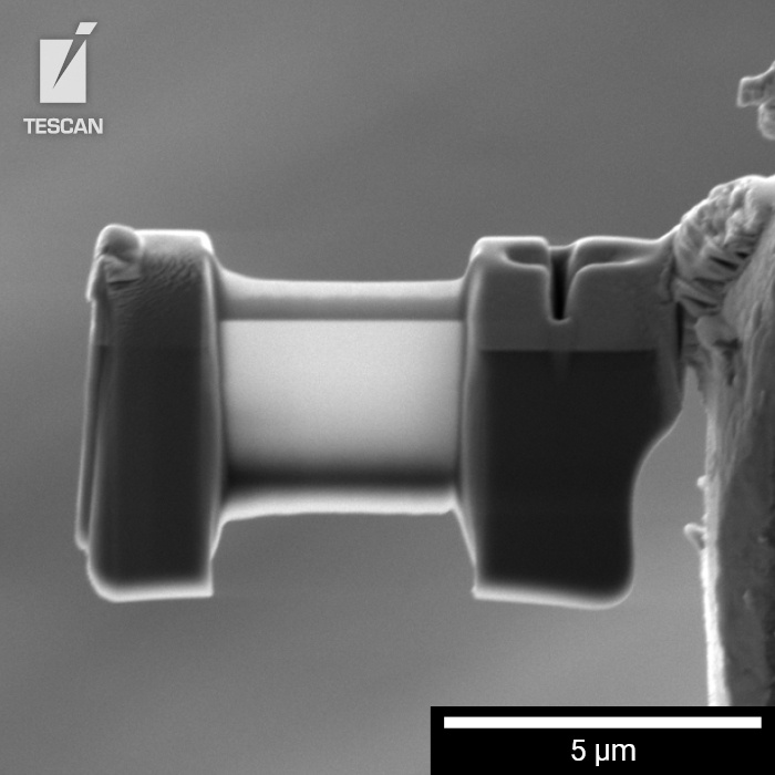
Prepare high-quality, damage-free TEM samples using the inert Xe ions of the Plasma FIB beam, avoiding Ga implantation or surface damage.
Artefact-Free
Cross-Sections

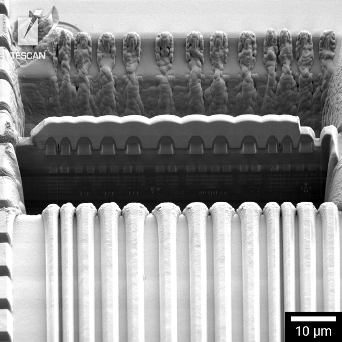
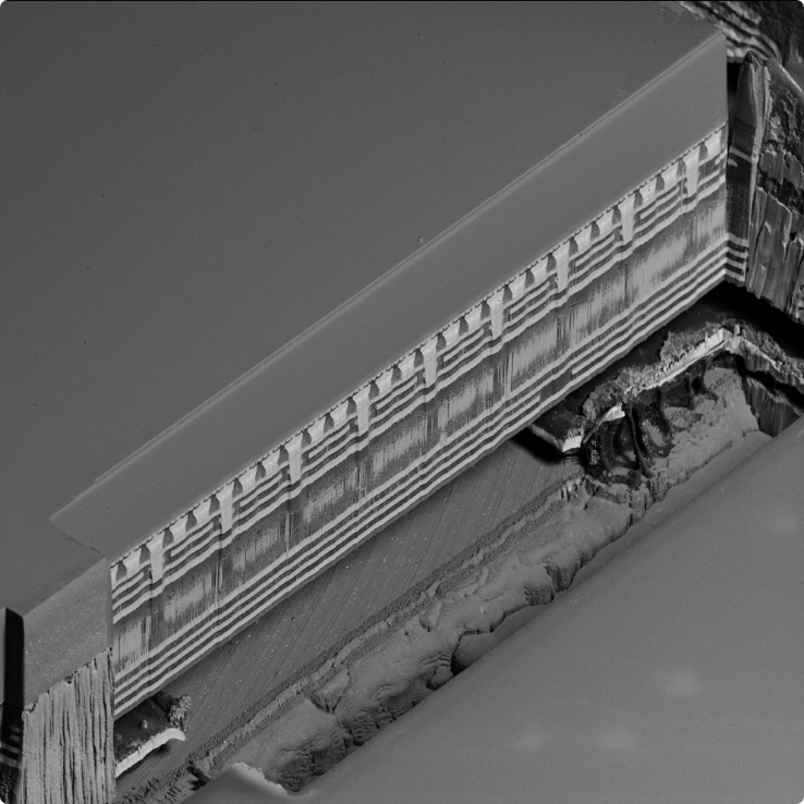
Create clean, artifact-free cross sections, even on challenging materials, using our patented Rocking Stage for alternating milling angles and TRUE X-sectioning for optimal ion beam use at high currents.
Register for Our Webinar to Discover More about TESCAN Plasma FIB-SEM
Analyze Complex Failures in Next-Gen IC Packages and Devices
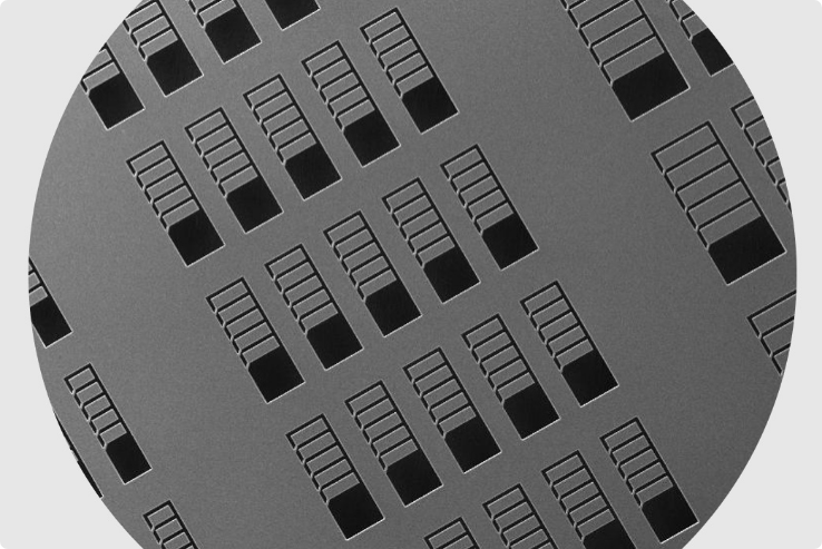
TESCAN SOLARIS X 2 excels in the physical failure analysis of advanced stacked IC packages (2.5D, 3D IC), flip-chips, MEMS devices, OLED and TFT displays, MLCC capacitors, 3D NANDs, and more.

Uncover Sub-Surface Features: Precision Ga-Free TEM Lamellae for STEM Analysis
Produce high-quality, Ga-free TEM lamellae under 100 nm thick from package and IC-level samples, ideal for subsequent STEM analysis.

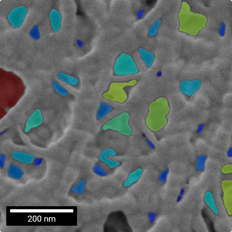
Unveil Material Secrets with In-Depth 3D EDS & EBSD Microanalysis
Leverage fast, large-volume 3D EDS and EBSD microanalysis for advanced packaging devices such as solder balls, TSVs, and bond pads, enabling comprehensive material composition analysis and characterization.
Key Benefits of TESCAN SOLARIS X 2
Localized Failure Analysis
Perform highly localized sub-mm scale physical failure analysis with the Mistral™ Xe Plasma FIB column, delivering maximum ion beam currents up to 3.3 µA for rapid material removal.
Artifact-Free Cross Sections
Produce clean cross sections free of curtaining and terrace artifacts, even on difficult materials like polyimide, SiC, ceramics, and glass, with our integrated Rocking Stage and TRUE X-sectioning technology to optimize milling angles and suppress ion beam tails.
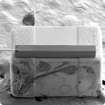
High-Quality Ga-Free TEM Lamellae
Prepare Ga-free TEM lamellae from semiconductor samples with improved quality and efficiency using Mistral’s enhanced ion beam profile, allowing the use of higher ion beam currents without compromising sample protection layers.


Precision End-Pointing
Achieve precise targeting of specific regions or defects (cracks, voids, delaminations) during milling or cross-sectioning with high resolution Triglav™ SEM imaging at the FIB-SEM coincidence point.


Maximized Throughput and Readiness:
Ensure consistent results and reduce setup times with fully automated electron column and Xe Plasma FIB column alignments.
User-Centric Productivity:
Increase productivity for all users with TESCAN’s advanced workflows and guided wizards in the Essence™ graphical user interface.
Boost your analyses with these solutions
TESCAN Rocking Stage
Achieve Artifact-Free FIB Cross-Sectioning and Precise SEM End-Pointing for Challenging Samples.
TESCAN True X-Sectioning
Save time with ripple-free plasma FIB cross-sectioning that doesn't compromise the high beam current advantage.
.