TESCAN TENSOR
Precise Analytical 4D-STEM Instrument
for Semiconductor Analysis
White Paper
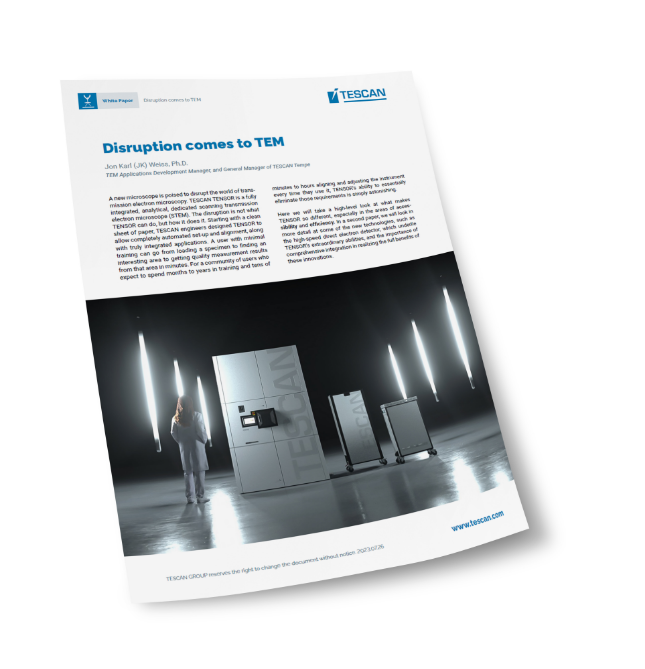
Disruption comes to TEM
Optimize your strain engineering, failure analysis, and process development with TESCAN TENSOR’s multimodal, precession-assisted 4D-STEM technology. Achieve precise structural and compositional characterization of advanced semiconductor devices faster, and with accurate results
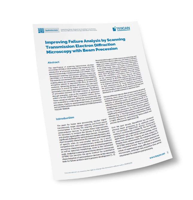
Application Note
Phase-Orientation Analysis of a PCM Device
For advanced semiconductor devices like phase change memory modules, TESCAN TENSOR enables precise structural failure analysis.
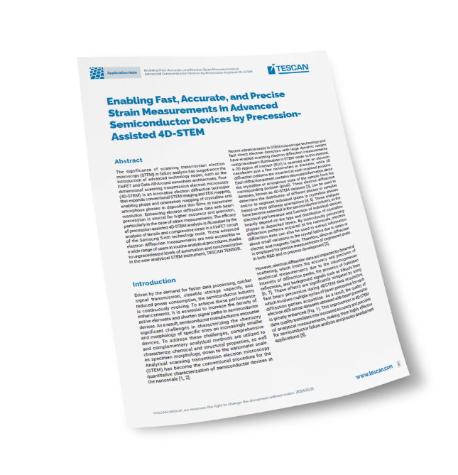
Application Note
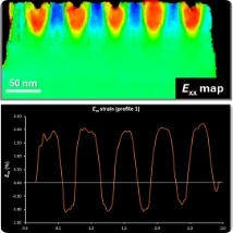
Strain Analysis in a 5-nm FinFET circuit
TESCAN TENSOR can perform precise strain measurements across large sample areas in complex semiconductor devices, such as 5-nm FinFET circuits or GAA nanosheets.
Application Note
Benefits of hybrid-pixel direct detectors for 4D-STEM
In developing the TENSOR, TESCAN engineers started with a clean sheet of paper to design a dedicated analytical STEM instrument optimized for 4D-STEM measurements that would deliver performance and usability far beyond that available from retrofits to legacy designs.
Enhanced Data Quality with Electron Beam Precession
Beam precession improves diffraction data quality by reducing dynamical scattering, resulting in highly precise and accurate measurements. This enhancement is essential for precise strain engineering in FinFETs and nanosheet gate-all-around transistors, as well as for accurate phase orientation analysis of multiphase semiconductor materials, such as hafnium zirconium oxide (HZO) or indium gallium zinc oxide (IGZO).
Fast precession of the tilted electron beam during acquisition of diffraction patterns at each pixel of a 4D-STEM dataset reduces dynamical scattering effects in the collected data, leading to more precise and accurate results:
- Diffraction patterns better correspond to precalculated kinematical templates used for template matching in phase and orientation mapping.
- An increased number of diffraction spots in the collected diffraction patterns improves the accuracy of template matching in phase and orientation mapping.
- More uniform intensity of individual diffraction spots increases the precision of their central position determination, which is critical for strain and other center-of-mass based applications.
Fully Automated Microscope Alignment for Seamless Operation
In TESCAN TENSOR, all microscope alignments are fully automated, eliminating the need for frequent manual adjustments of illumination conditions, beam scanning, and data collection. The electron beam’s precession is perfectly aligned with the specimen surface, ensuring the smallest possible spot size for optimal spatial resolution.
This level of automation means that no daily, weekly, or monthly adjustments are needed for different STEM imaging, EDS mapping, or diffraction modes. TESCAN TENSOR is always ready for high-quality data collection at optimal optical settings, with fast and seamless switching between the different analytical modes.
Simplified Specimen Tilting for Strain and Defect Analysis
TESCAN TENSOR’s automation makes tilting the specimen to the zone axis intuitive, simplifying complex tasks such as strain measurement or defect imaging (e.g., stacking faults or dislocations). This streamlines in-session operations and ensures accurate measurements for advanced semiconductor analysis.
Accelerated 4D-STEM Data Collection and On-the-Fly Analysis
TESCAN TENSOR’s high-speed beam precession reduces acquisition times by up to 10 times, allowing 4D-STEM datasets to be captured in minutes instead of hours.
In addition, on-the-fly data processing delivers maps within minutes during the data collection session, eliminating the need for extensive data transfers and post-processing. This enables faster decision-making in your analysis workflow.
No Data Degradation with Near-UHV Sample Conditions
TESCAN TENSOR ensures reliable and repeatable measurements from the same region of interest without signal deterioration caused by hydrocarbon contamination, even under high beam currents used for EDX (Energy Dispersive X-ray Spectroscopy) mapping. By operating at near-UHV (ultra-high vacuum) levels, hydrocarbon contamination is prevented and sample quality preserved across multiple performed analyses.
Unlike traditional systems, TESCAN TENSOR maintains these conditions without cooling by liquid nitrogen, reducing system downtime for otherwise needed cryo-cycles. Moreover, it provides safer microscope operation and minimizes operator safety training requirements. This enables uninterrupted 24/7 operation, maximizing system uptime for semiconductor analysis.
Improved Throughput and Faster Results
TESCAN TENSOR significantly enhances throughput by eliminating the need for regular manual alignments and accelerating data acquisition. The integration of dual 100 mm² SDD sensors provides a high signal collection solid angle of 2.0 sr, while the usage of 100 kV acceleration voltage results in superior X-ray signal generation.
The hybrid-pixel, direct electron diffraction detector (Dectris Quadro) offers a high dynamic range (~107), rapid acquisition (up to 4,500 fps), and exceptional sensitivity using the electron counting mode for diffraction data collection.
Combined, these features enable a 10-fold increase in analysis speed for multimodal sample characterization.
How TESCAN TENSOR Meets Your Analytical Needs
Purpose-Driven Performance
Accelerate nanoscale structural and compositional analysis using high-speed, precession-assisted 4D-STEM.
Next-Level
Precision
Perform reliable strain measurements and phase orientation analysis with enhanced diffraction data quality and perfectly aligned microscope optics.
Automated, Sample-Focused Interface
Spend more time on analysis and less time on microscope adjustments, thanks to TESCAN’s ExploreTM interface and automated workflows.
Real-Time, Interactive Data Processing
Analyze 4D-STEM datasets directly at the microscope with on-the-fly data processing, delivering clear, actionable results during data collection.
Reproducibility Without Operator Dependence
Consistently obtain reliable results with fully automated alignments and preset acquisition settings, independent of the user’s skill level.
Minimal
Sample
Contamination
Conduct multiple analytical STEM measurements without degradation, thanks to near-UHV sample environments.
Integration
into Your Existing Protocols
Seamlessly export precession-assisted 4D-STEM data in standard formats for easy integration into established workflows.
Fast training
of new
operators
Onboard and train new users quickly thanks to TENSOR’s advanced automation and intuitive operation.
Real-World Applications of TESCAN TENSOR
in Advanced Semiconductor Analysis
A case study of a 22-nm device node
TENSOR provides high-quality EDS data using its dual 100 mm² detectors placed near the sample, enabling a total collection solid angle of 2.0 sr. With 100 keV energy and electron beam currents up to 10 nA at a 1 nm beam size, EDS maps are captured in just minutes, as opposed to the typical half-hour.
Additionally, TESCAN TENSOR’s rapid switching between STEM imaging and EDS mapping without manual alignments enhances throughput in these routine measurements.
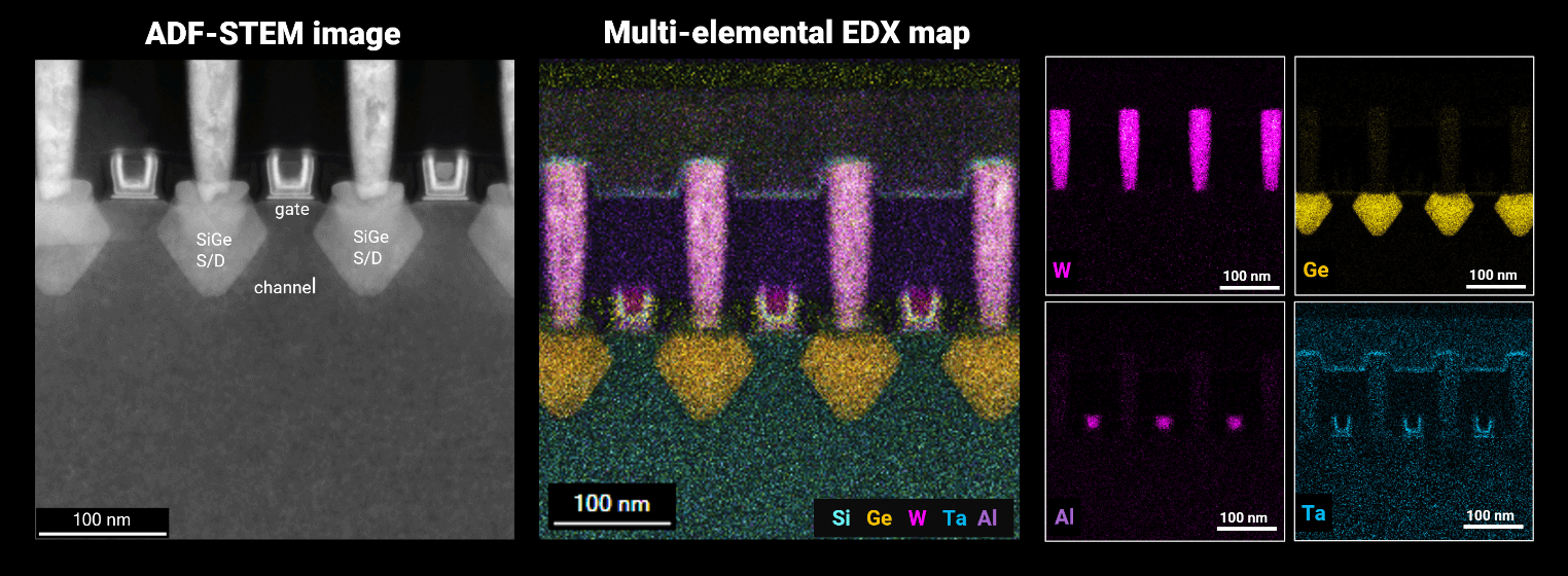
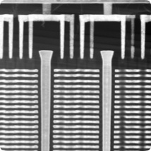
Routine Characterization of Semiconductor Devices: A Case Study of 3D NAND Cells
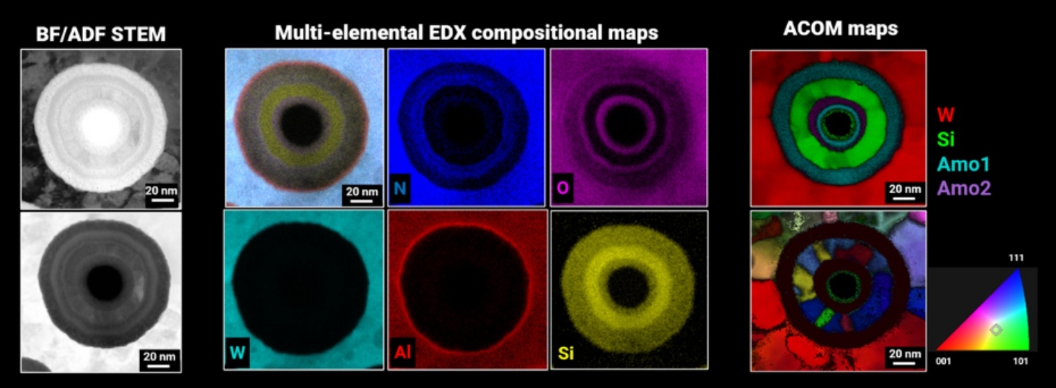
TESCAN TENSOR’s windowless EDS detectors, combined with high beam currents and 100 kV acceleration, produce strong signals even for light elements such as carbon, nitrogen, and oxygen. This capability is particularly beneficial for small devices like 3D NAND cells.
The EDS analysis can be further augmented by 4D-STEM phase and orientation mapping (ACOM), which integrates seamlessly into the system’s automated workflows, allowing for enhanced characterization with minimal user effort.
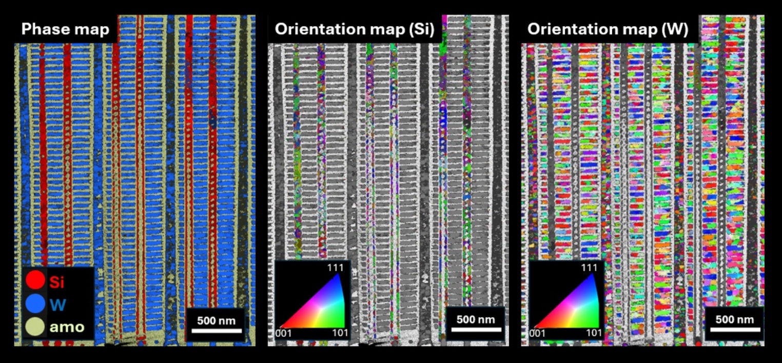
Grain Size Distribution in Multiphase Nanodevices: A Case Study in 3D-NAND Devices
TESCAN TENSOR simplifies grain size distribution analysis in complex, multiphase devices. Its fast beam precession and real-time data processing enable rapid, accurate determination of phase and grain structure
across large regions of stacked VNAND devices, delivering results in a fraction of the time in comparison with the traditional TEM/STEM instruments.
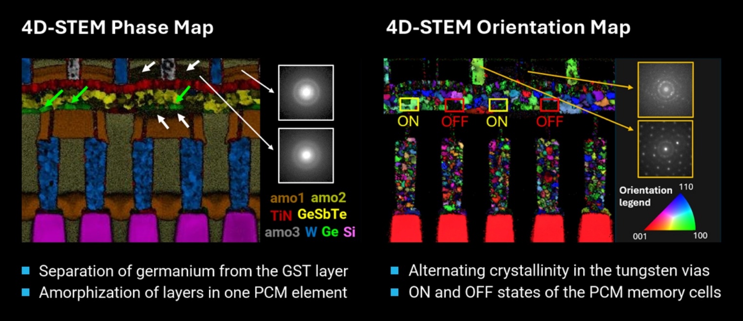
Enhancing Failure Analysis with 4D-STEM: A Case Study of Phase Change Memory
For advanced semiconductor devices like phase change memory modules, TESCAN TENSOR enables precise structural failure analysis. By unambiguously identifying defects such as germanium separation or amorphization in layers and vias, you can diagnose and address failure points with confidence.
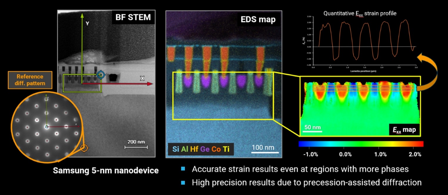
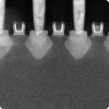
2D Strain Analysis in Semiconductor Devices: A Case Study of 5-nm FinFET Circuits
TESCAN TENSOR can perform precise strain measurements across large sample areas in complex semiconductor devices, such as 5-nm FinFET circuits or GAA nanosheets. The precise beam-precession alignments, unrestricted speed of data acquisition, and proprietary strain calculation algorithm ensure high accuracy and precision, helping optimize strain engineering and improve device performance.
Key Benefits of TESCAN TENSOR for Semiconductor Analysis
TESCAN TENSOR delivers a comprehensive set of analytical capabilities designed to enhance the accuracy, efficiency, and reproducibility of semiconductor device characterization.
Standard Analytical Techniques
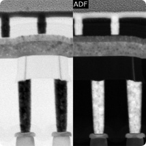
Benefit from powerful imaging modes including Bright Field (BF), Dark Field (DF), and High-Angle Annular Dark Field (HAADF) STEM imaging, along with precise EDS (Energy Dispersive Spectroscopy) elemental mapping.
New Characterization Capabilities
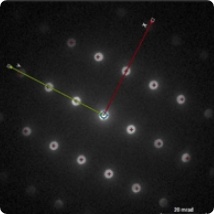
Leverage advanced electron diffraction techniques with precession-assisted 4D-STEM for precise strain and phase mapping, opening new avenues for semiconductor analysis.
Enhanced Data Quality
Electron beam precession, combined with a 100 kV acceleration voltage, improves diffraction and EDS data quality, enabling more accurate and detailed measurements.

Interactive and Real-Time Operation
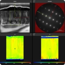
On-the-fly data processing delivers results already during the measurement process, allowing for immediate interpretation and faster decision-making.
Faster Time to Multimodal Results
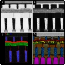
Rapid data acquisition and seamless switching between analytical modes boost throughput, reducing the time needed for comprehensive sample characterization.
Reproducibility and Consistency
Predefined data acquisition presets ensure reproducible results with high yield, regardless of the operator’s experience level.
Uncompromised Reliability
Full automation of microscope alignments guarantees optimal results without requiring user intervention, ensuring consistent performance every time.
Minimal Sample Deterioration
Near-UHV (ultra-high vacuum) conditions prevent hydrocarbon contamination, maintaining sample integrity over multiple high-current measurements.
Elevate Your Semiconductor Characterization with TESCAN TENSOR
TESCAN TENSOR transforms routine multimodal characterization by incorporating structural insights obtained through advanced electron diffraction techniques. The system delivers enhanced accuracy, precision, and reproducibility for phase orientation mapping and strain measurements.
Speed up your analysis with automated microscope alignments, fast switching between STEM and EDS modes, and real-time data analysis that eliminates the need for post-processing. Beam precession ensures high-quality diffraction data, further boosting measurement precision.
TESCAN TENSOR makes advanced STEM measurements accessible to all users with streamlined workflows, predefined optical settings, and easy-to-use interfaces - empowering your lab to achieve more, faster, and with greater confidence in your results.
Questions?
Want a virtual demo?
Our global team is ready to answer questions about TESCAN FIB-SEMs and our solutions for Semiconductors and IC Packaging Failure Analysis.

