TESCAN invites you to join us at
Microscopy & Microanalysis 2023 in Minneapolis, Minnesota
from July 24-27, 2023
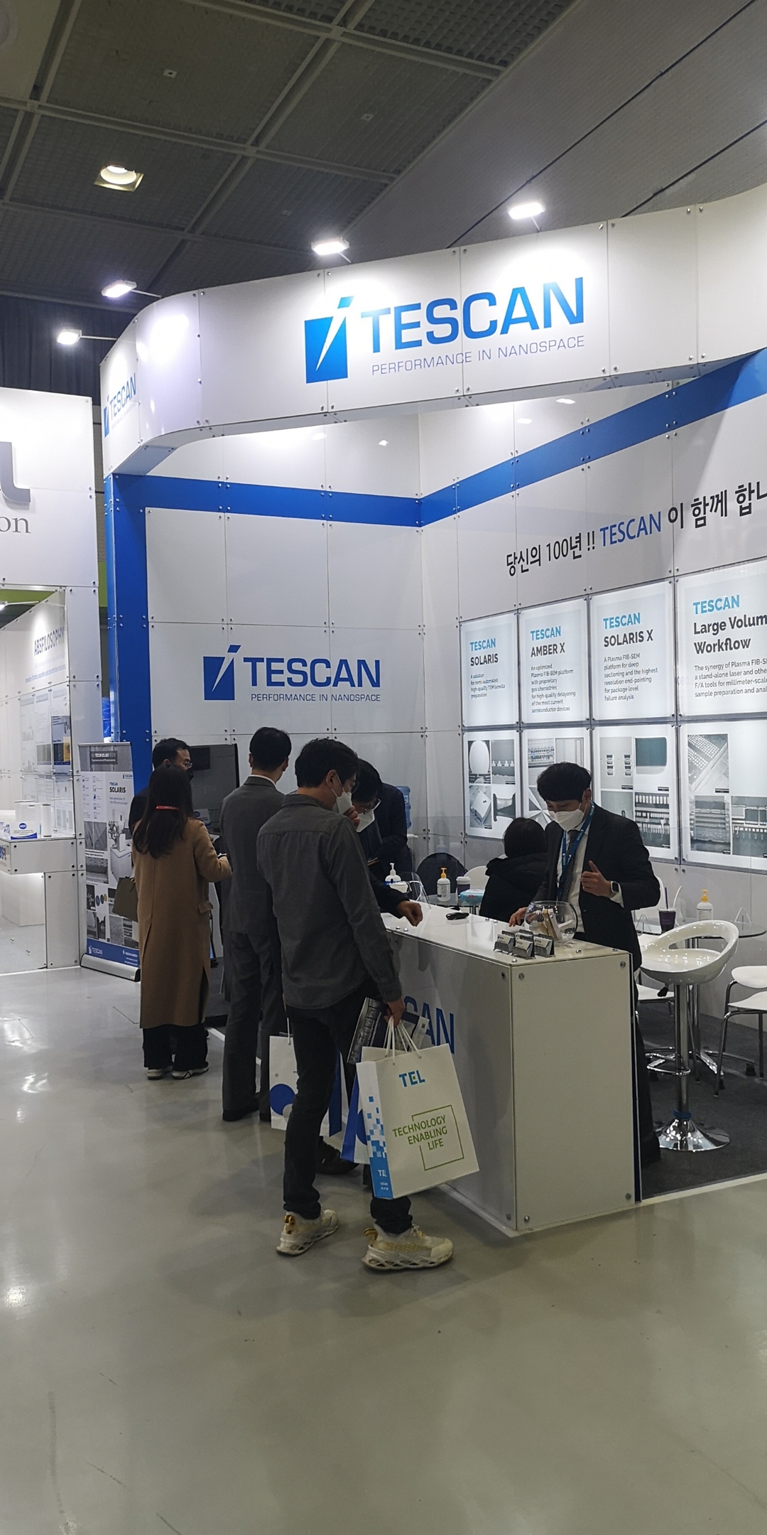
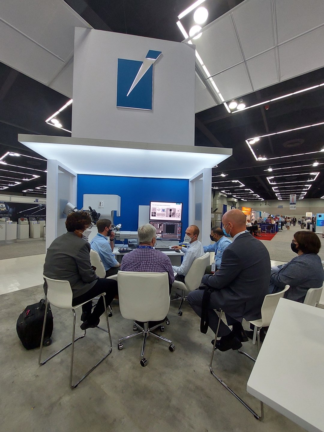
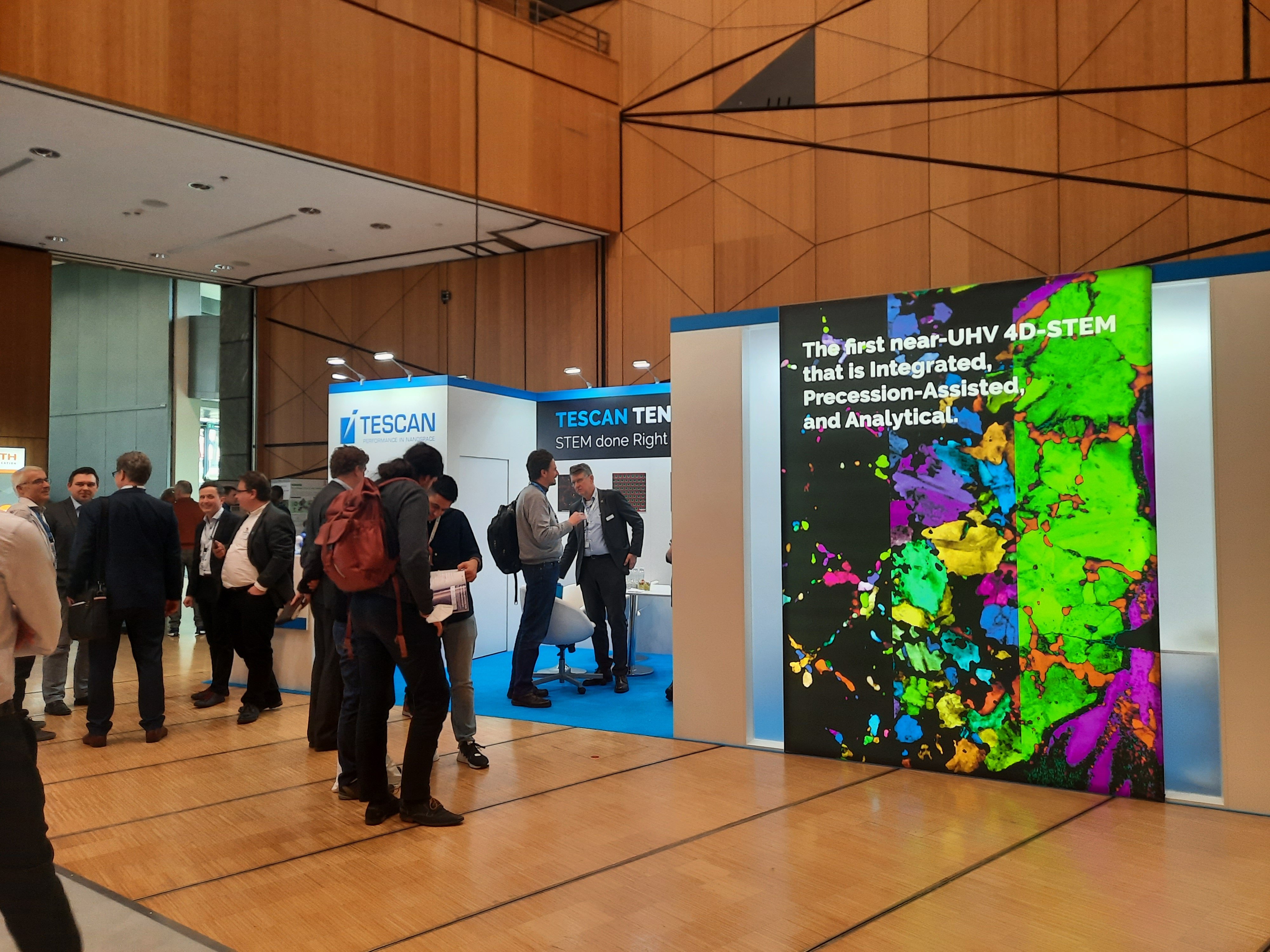
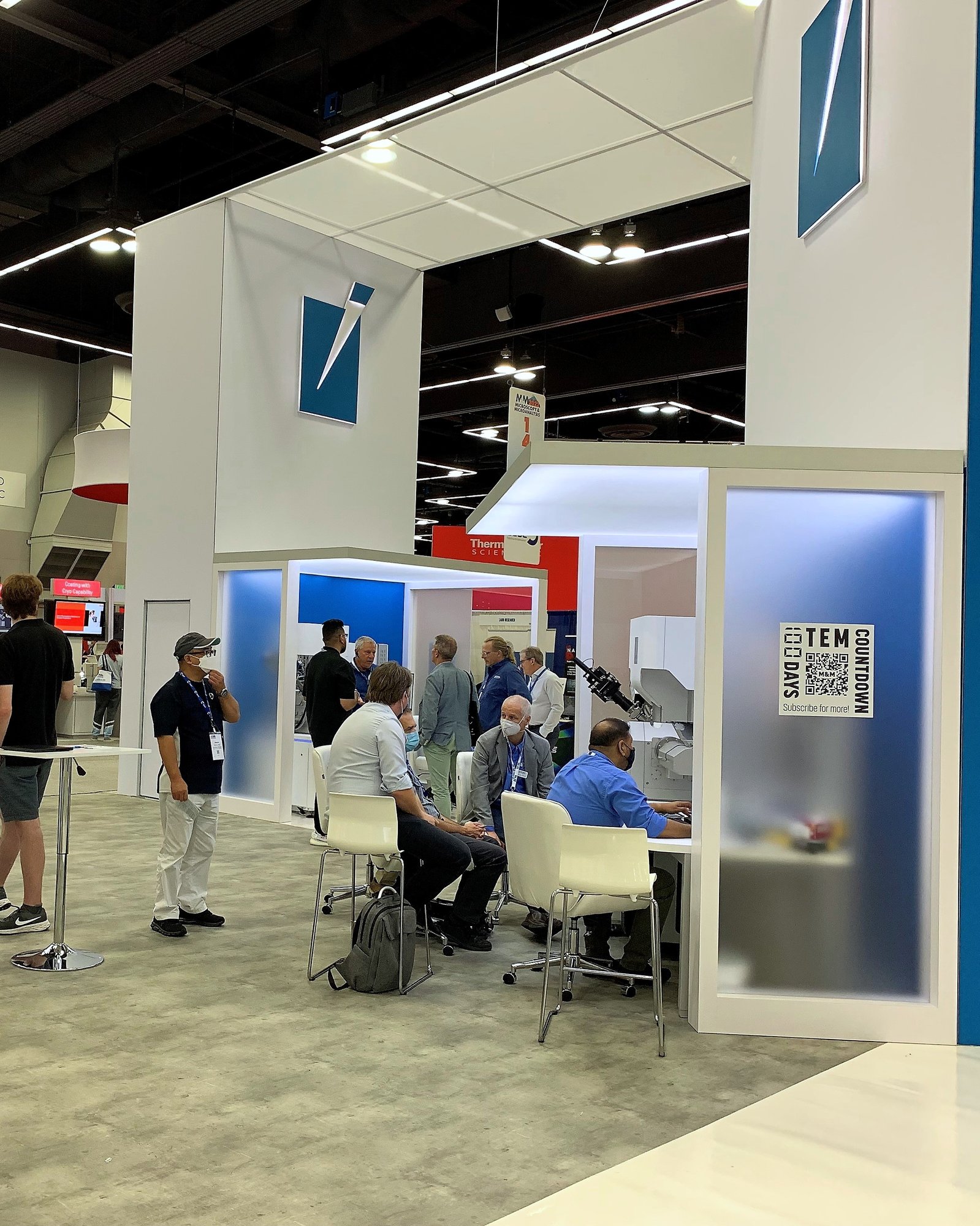
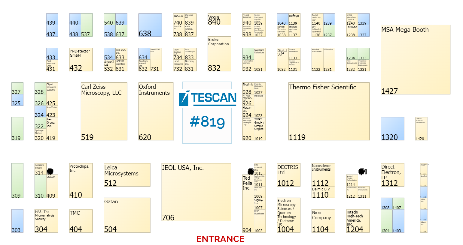
The TESCAN Global Team is excited to meet you at BOOTH 819 during M&M 2023 in Minneapolis. Our full list of scientific talks, in-booth presentations, and demo opportunities are listed below. Please make sure to register in advance for our in-booth activities, space is limited!
Opportunities to explore and experience TESCAN during M&M 2023 include:
- Demo TESCAN TENSOR 4D-STEM, our fully integrated, precession-assisted, analytical 4D-STEM, is designed to address the needs of anyone with an interest in multimodal nano-characterization applications (morphological, chemical, and structural), including materials scientists, semiconductor R&D, failure analysis engineers, and crystallographers
- Demo on the newly upgraded TESCAN CLARA UHR-SEM, our versatile UHR microscope solution for providing maximum detail and contrast information from any sample—even magnetic and beam-sensitive materials
- The TESCAN UniTOM HR will be showcased, as a versatile micro-CT system that combines high spatial resolution with a high temporal resolution that is optimized for static and dynamic imaging, fulfilling all of the necessary imaging requirements
- Learn how the TESCAN AMBER X FIB-SEM can drive your product development and get comprehensive answers fast and effortless
Don't miss out on this unique opportunity to learn and explore the latest advancements in microscopy. We look forward to seeing you at BOOTH 819!
Register for Demonstrations
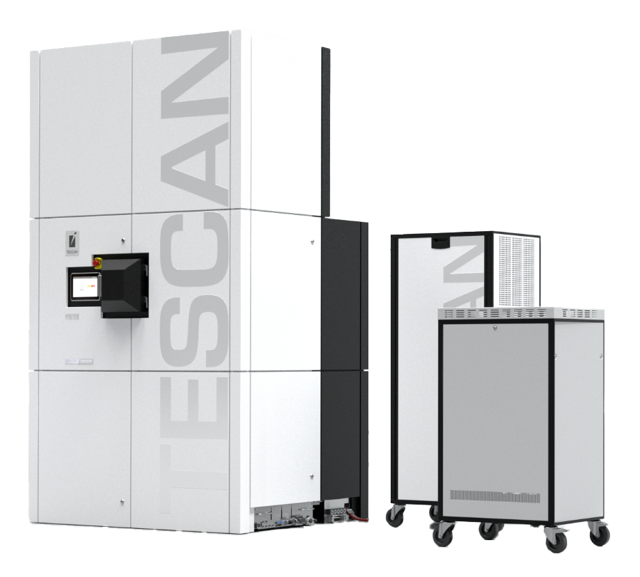
TESCAN TENSOR
Experience an exclusive TENSOR demo. The first near-UHV 4D-STEM.
TESCAN TENSOR
Online reservations are now closed. Please visit us at booth 819 to register for demos. Thank you!
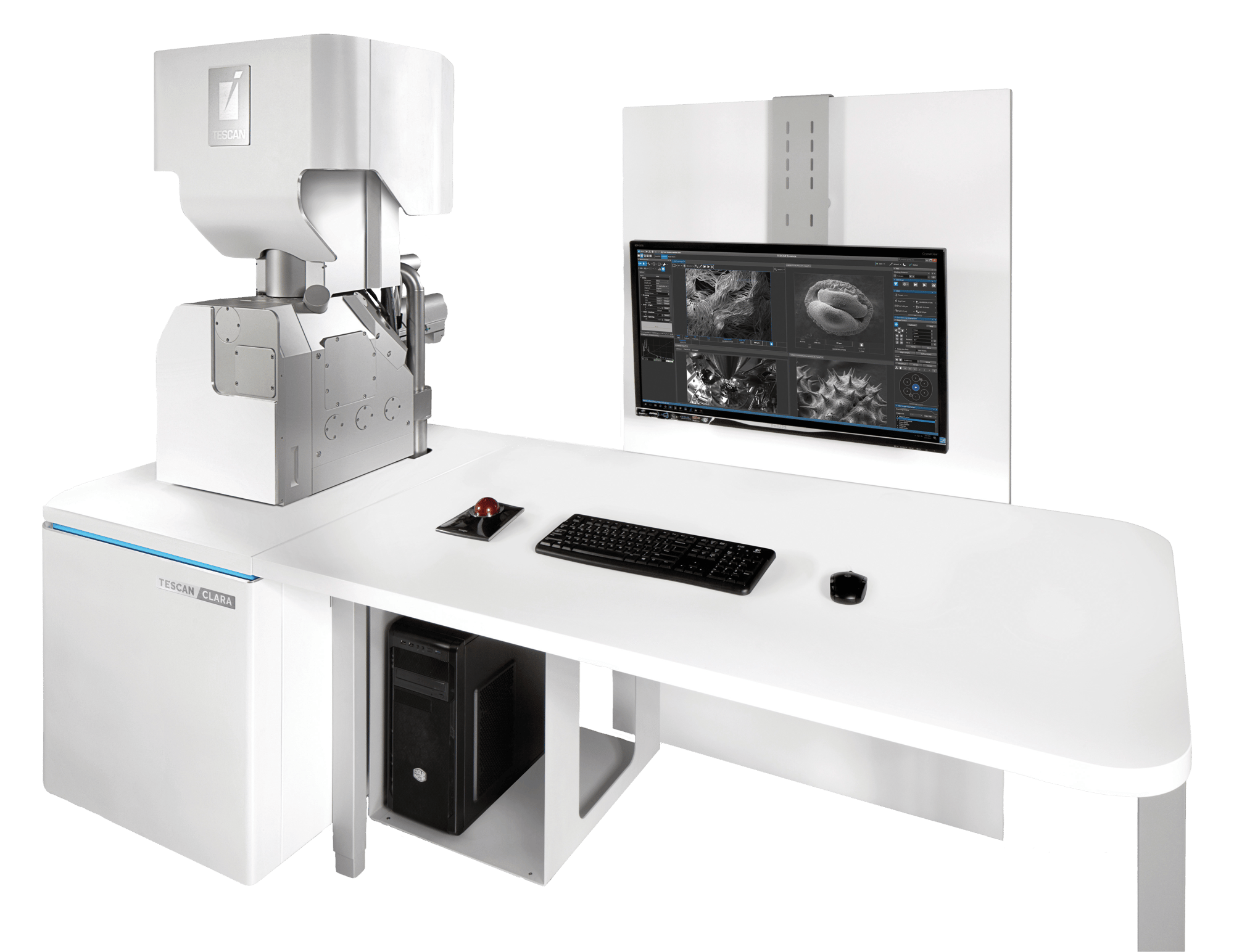
TESCAN CLARA
UHR SEM for fast, accurate, and comprehensive nanoscale surface analysis of any material
TESCAN CLARA
Online reservations are now closed. Please visit us at booth 819 to register for demos. Thank you!
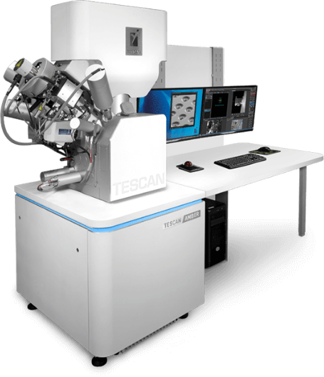
TESCAN AMBER X
A unique combination of Plasma FIB and field-free UHR FE-SEM for multiscale materials characterization.
TESCAN AMBER X
Online reservations are now closed. Please visit us at booth 819 to register for demos. Thank you!
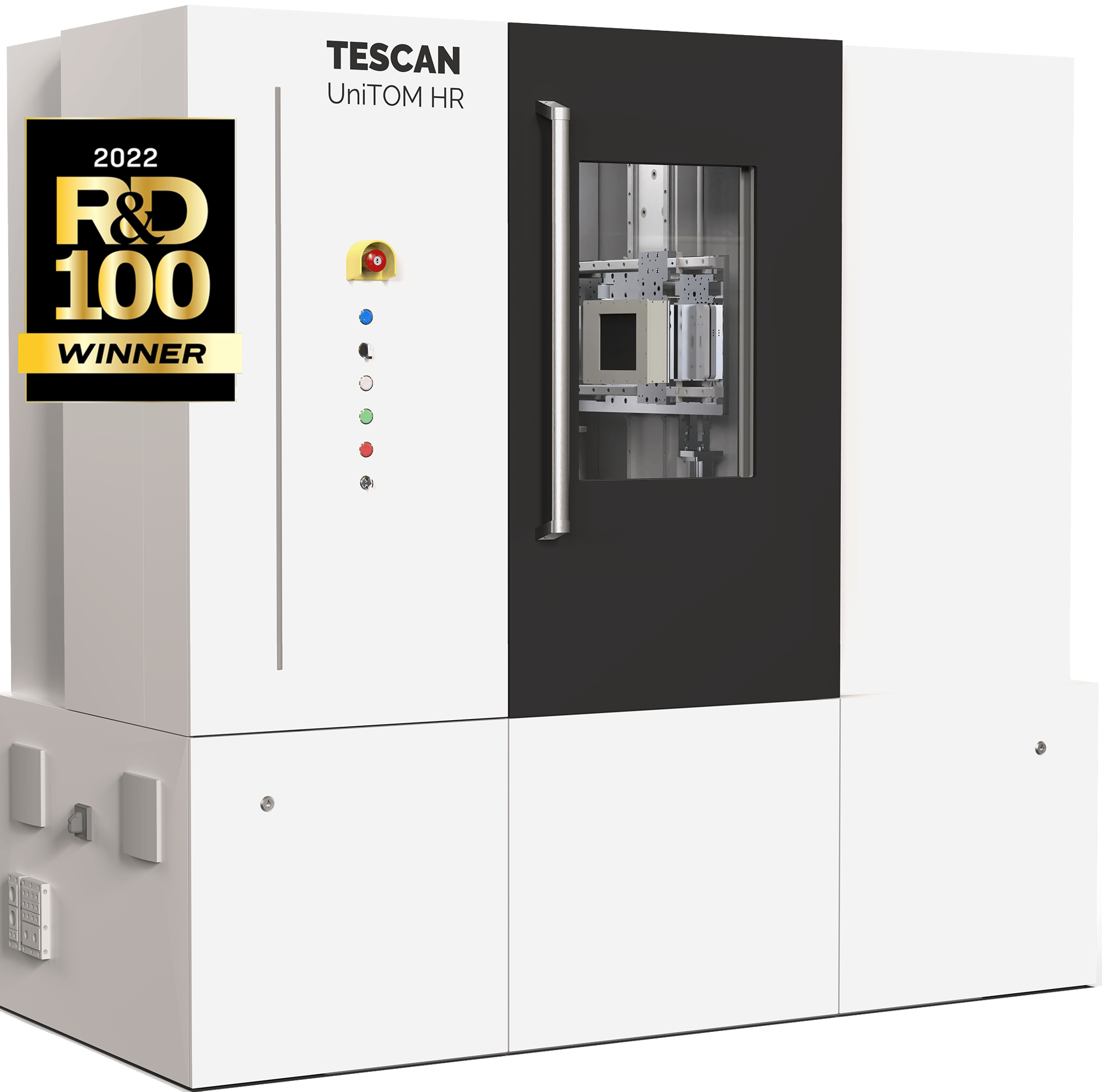
TESCAN UniTOM HR
The first micro-CT system to provide sub-micron spatial resolution and high temporal resolution dynamic CT in a single, highly-versatile system.
TESCAN UniTOM HR
Online reservations are now closed. Please visit us at booth 819 to register for demos. Thank you!
Booth Presentations
ACCELERATING CRYO-TEM SAMPLE PREPARATION
Cryo-electron tomography (cryo-ET) has revolutionized structural biology by enabling the observation and characterization of biological samples at a molecular level in their near-native state. This technique provides an unprecedented level of structural detail, but it necessitates thin specimens (typically below 200nm) for effective electron beam penetration. Presently, the prevailing method for achieving such thinning involves Focused Ion Beam (FIB) milling. FIB instruments utilizing Gallium ion sources are widely employed, offering exceptional resolution and precise milling. However, the meticulousness of sample preparation becomes time-consuming, creating a bottleneck that restricts overall lab throughput.
Recently, there has been a surge of interest in adopting FIBs based on plasma ion sources to expedite cryo transmission electron microscopy (TEM) lamella preparation. Commonly employed ion sources include Xenon, Oxygen, and/or Argon. Among these options, Xenon stands out as the most suitable choice due to its highly focused beam profile, which facilitates precise lamella shaping and accelerates the milling rate.
In the lecture, we will delve into the practical advantages of optimized workflows, specifically focusing on on-grid lamella, waffle, and lift-out techniques, aimed at enhancing the speed and throughput of cryo-TEM lamella preparation. Furthermore, we will explore the TESCAN AMBER X cryo-plasma FIB-SEM as a robust and versatile workstation that serves as an indispensable tool for routine cryo-TEM sample preparation. This instrument not only excels in its primary function but also offers a remarkable range of additional capabilities, making it a comprehensive solution for various research needs.
Registration Form
VENDOR TUTORIAL: ACCELERATING AND ADVANCING NANOSCALE CHARACTERIZATION OF MATERIALS BY SEAMLESS 4D-STEM WORKFLOWS USING THE NEW TESCAN TENSOR ANALYTICAL STEM MICROSCOPE
The new scanning transmission electron microscope, TESCAN TENSOR, is changing the way how materials can be characterized at the nanoscale by enabling precise analyses of morphological, chemical, and structural properties of various samples at ease to all users, including material scientists, semiconductor technicians, and STEM method developers. The performance and usability of analytical 4D-STEM techniques are not compromised by the design of TEM microscopes that were not intrinsically designed for analytical STEM applications anymore. In the design of this new analytical STEM microscope, we integrated state-of-the-art components such as a large direct electron detector with hybrid pixel technology, electron beam precession, electrostatic beam blanker, and large dual EDS detectors. Ultra-high vacuum engineering then provides near ultra-high vacuum at the specimen area and negligible hydrocarbon contamination from the column. Full integration of all these components facilitated their precise synchronization and improvement in their performance and overall throughput of STEM, EDS, and 4D-STEM measurements. Controlled from a single user interface that provides a seamless user experience, acquired data can be processed and analyzed on the fly and visualized almost in real-time, making sample characterization an interactive experience instead of batch data acquisition and later post-processing.
A novel approach to analytical STEM measurements has enabled the simplification of sample analysis workflows that do not require TEM imaging and switching between TEM and STEM modes. Advanced on-the-fly automation of system alignments and adjustments of STEM imaging, STEM analysis, and 4D-STEM nanobeam settings enables user experience comparable to SEM and FIB/SEM instruments. Users can therefore focus and spend precious instrument time on the interaction with the specimen, whilst minimizing time spent on the electron column adjustments and alignments. This new approach supports enhanced system accessibility, utilization, and productivity, for a wide range of users without weeks, if not months, of prior training or experience in using complex high-end TEM equipment. At the same time, experienced users can customize measurement conditions, export 4D-STEM data to open-source computational platforms (such as LiberTEM, HyperSpy, or pystem), or develop their own custom measurements with the ExpertPI interface for their own experiments and workflows.
In summary, the new analytical STEM microscope provides analytical STEM, EDS, 4D-STEM, and tomography capabilities catering to a wide range of experiments that find applications in the multimodal, nanoscale morphological, chemical, and structural characterization of functional materials, thin films, and synthetic and natural crystals.
Registration Form
XE ION MILLING IN AN OXYGEN-RICH ENVIRONMENT: A POSITIVE EXPERIENCE
Dr. Ford will discuss how introducing oxygen near the sample surface with a direct gas injection system during Xe plasma milling can minimize curtaining and redeposition artifacts in a variety of polymer nanocomposites and biological tissue samples.
Registration Form
(COLOR) X-RAY COMPUTED TOMOGRAPHY FOR MANUFACTURING
X-ray Computed Tomography (XCT) has become ubiquitous in manufacturing given its unique ability to see inside objects. Previously destructive tear downs and sectioning would have been required to identify defects and anomalies, rendering the parts unusable. There is a strong desire to incorporate this into manufacturing lines given its non-destructive capability to recognise issues at various stages in the process, however depending on the part this can take 10’s of minutes to hours. One route out of this problem is through advanced reconstruction where one can acquire relatively limited data and achieve the same quality result but at a fraction of acquisition time. Current systems utilise absorption only techniques that show the user the relative density of the parts, but the advent of spectral or “color” CT looks to add further layers to non-destructive testing by providing elemental information about inclusions and material makeup. In this talk I discuss the uses of XCT at WMG, University of Warwick with respect to manufacturing, what we are doing to tackle this speed issue, and an eye on future spectral exploitation.
Registration Form
ADVANCING STRAIN ANALYSIS BY USING NANOBEAM 4D-STEM MEASUREMENTS
Continuous development of new materials and semiconductor devices is driven by the demand for materials with improved mechanical properties as well as for nanotechnology facilitating faster data processing, faster signal transmission, greater storage capacity, and continuously decreasing power consumption. Consequently, material scientists and semiconductor manufacturers are challenged when characterizing chemistry and morphology at specific sites at the nanoscale. 4D-STEM is a powerful analytical technique based on nanobeam diffraction that can resolve and characterize the distribution of crystalline phases and orientations of individual grains in polycrystalline materials and different layers of semiconductor devices at the nanoscale level. However, the broader adoption of 4D-STEM techniques has been limited by the complexity of experimental setups and challenges with synchronization of sample scanning by an electron beam with beam blanking, beam precession, and readout of a pixelated detector. In this presentation, we will show a new approach to the acquisition and processing of 4D-STEM datasets quickly and with minimal user input due to the full integration of all needed hardware components with high levels of system automation and optimization algorithms for on-the-fly data processing and visualization of results.
The power of 4D-STEM characterization will be demonstrated in quantitative analysis and visualization of Lagrange strain in user-defined tensile directions, shear, and pattern rotation at the interface between different material layers. A 4D-STEM strain map taken from a Si0.8Ge0.2 epitaxial film on a silicon substrate displayed a tensile strain within the gradient at the interface between the silicon and Si0.8Ge0.2 layer with respect to the silicon substrate. The strain values were calculated based on a user-defined reference pattern from an unstrained region using a fully automated procedure with on-the-fly data processing, which is accessible to all operators of analytical instruments. Additionally, the power of 4D-STEM measurements using nanobeam electron diffraction will be demonstrated on strain measurement in polycrystalline materials and grains as small as ~50 nm in diameter. Finally, the selection of electron acceleration voltage and performance of 4D-STEM measurements at 100-kV acceleration will be discussed.
Registration Form
MULTIMODAL CHARACTERIZATION IN THE EVALUATION OF ELECTROCHEMICAL MATERIALS AND THEIR INTERPHASES
Electrochemical materials in battery designs and research on them are critical in achieving a sustainable energy future as well as energy independence from fossil fuels. In practice, energy density, cell longevity, and charge rate are bonded to chemical composition and specific structural features within the batteries. In general, optimization of all these parameters is a multiscale, multimodal challenge that consists of analysis of the anode, cathode, electrolyte, and their interphases. In this presentation, we focus on characterization techniques and their usage that offer critical insight to optimize battery performance and lifetime.
Registration Form
IMPROVING 4D-STEM PHASE AND ORIENTATION MAPPING AT THE NANOMETER SCALE
Phase and structural characterization at the nanoscale play an essential role in the development of new materials with improved physical and mechanical properties as well as in the development and quality assessment of increasingly smaller semiconductor devices.
Analytical 4D-STEM is a powerful analytical method based on nanobeam diffraction that can resolve and characterize the distribution of crystalline phases and orientations of individual grains in polycrystalline materials at the nanoscale level. These analyses are critical because physicochemical, electrical, and mechanical properties strongly depend on the distribution of crystalline grains and interfaces between different phases in prepared materials or annealed semiconductor devices. However, the broader adoption of 4D-STEM techniques has been limited by the complexity of experimental setups and challenges with synchronization of sample scanning with electron beam blanking, precession, and detector readout. In this presentation, we will show a new approach to the acquisition and processing of 4D-STEM datasets quickly and with minimal user input due to the full integration of all needed hardware components with high levels of system automation and optimization algorithms for on-the-fly data processing and visualization of results.
The power of 4D-STEM characterization will be demonstrated on the identification of phases in a semiconductor device that contained anomalies in the GST layer that could not have been revealed by using the standardly used analytical methods such as EDX elemental mapping. Additionally, improvements in accuracy and robustness of 4D-STEM phase analysis by using multi-modal analysis in combination with simultaneously acquired EDS data will be shown on an example of a polycrystalline aluminum foil with added gold nanoparticles which have very similar crystal structures (a lattice parameter difference of less than 5%). Finally, the advantages and performance of 4D-STEM measurements conducted at 100-kV acceleration using an optimized direct electron detector will be discussed for samples of a wide range of lamella thickness.
Acknowledgments
We are grateful to STMicroelectronics (Grenoble, France) for providing a semiconductor device for the multimodal phase and orientation analysis used in this study.
Registration Form
LARGE SCALE XE PFIB/SEM ANALYSIS OF SHALE: NANOMETER RESOLUTION ACROSS MILLIMETERS OF ROCK…WHAT IS STILL POSSIBLE?
The ability to analyze samples across the nanometre to millimetre range is critical for addressing many of today’s challenges in materials science, manufacturing and geology. In many cases, the challenges that samples present cannot be addressed using traditional Ga+ FIB-SEM as the milling rate is not sufficient for extra-large-scale milling experiments, especially for geological samples. This challenge is well addressed using Xenon plasma FIB, which allows to the removal of large volumes in a fraction of the time that Ga FIB/SEMs can.
Shale is a very fine-grained sedimentary rock with complex heterogeneous composition and anisotropic fabric. It is often laminated on the scale of hundreds to thousands of micrometres while consisting of micro- to nanometre-sized sheet silicates, tectosilicates, carbonates, and organic grains and particles, which have anisotropic shapes arranged in a shape-preferred orientation. To capture the compositional and geometric heterogeneity, shale samples usually must be analysed on the scales of several millimetres while resolving nanometre-sized grains and voids, ideally with methods that provide compositional and mineralogical information. This requirement poses a significant challenge to the microscopist.
This presentation demonstrates the use of a Xe-PFIB/SEM equipped with EDS and EBSD for the chemical and structural characterization of a typical shale sample. Like most shales, the examined sample is charging and brittle, which renders site-specific processing with cross-sectional EBSD analysis very challenging. The process of preparing millimetre-sized cross-sections and lifting out a large, site-specific rock cross-section as well as the road to success are discussed in detail and the achieved results compared to traditionally polished samples.
Figure 1: EBSD measurements of a shale cross-section which was prepared traditionally (top) and via Xe PFIB/SEM (bottom). The FSD images (left) show the achieved surface roughness of the techniques. The phase maps of different phases show the achieved EBSD quality for each preparation technique. The corresponding percentage of zero solutions (not indexed) is given next to the image.
The authors acknowledge the Central Analytical Research Facility at which the measurements were recorded using the ARC-funded TESCAN Xe-PFIB/SEM ‘S8000X’.
Registration Form
VENDOR TUTORIAL: STREAMLINING MATERIALS SCIENCE SAMPLE CHARACTERIZATION WITH HIGHLY AUTOMATED FIB-SEM TEM SAMPLE PREPARATION FOR ANALYSIS IN TESCAN TENSOR 4D-STEM
The presentation focuses on automated sample preparation for Transmission Electron Microscopy (TEM) using Focused Ion Beam Scanning Electron Microscopy (FIB-SEM) Solutions. Automation extends the accessibility of the TEM/STEM analysis to a wider Materials Science research base. Additionally, automation ensures consistent results by eliminating user-depended variations in the TEM lamella preparation process.
The TEM lamella preparation automation accommodates the diverse materials commonly encountered in materials research, allowing easy adaptation to different materials. The intuitive and fast adjustment of the specific material type-dependent milling properties to the widest range of material types enhances the effectiveness and versatility of automated TEM sample preparation. Furthermore, the quality of TEM samples significantly affects the accuracy of TEM/STEM materials characterization results. Minimizing deficiencies in TEM samples prepared in batches or from various materials contributes positively to the dependability of TEM/STEM analyses.
In this talk, we prove this by showcasing TEM samples prepared using an automated process by Essence Autoslicer™ consisting of fully automated FIB-SEM preparation and polishing steps on a variety of materials such as those based on silicon, metal alloys, ceramics, and thin coatings on a substrate. These samples were subsequently analyzed using the TESCAN TENSOR 4D-STEM system proving the best quality for TEM/STEM characterization.
Registration Form
M&M Scientific Program
ADDING ANOTHER DIMENSION TO 4D-STEM WITH EDX-ASSISTED CRYSTAL ORIENTATION AND PHASE MAPPING
4D-STEM crystal orientation and phase mapping is a powerful technique for the nanocharacterisation of materials, as it can provide simultaneous information on phase distributions, grain size, and crystal orientation. However, it can be challenging to separate phases with similar lattice parameters and symmetries (lattice parameter difference of <5%). EDX mapping can be used to separate phases with different chemical compositions but cannot provide crystal orientation information. A combined method leveraging both 4D-STEM and EDX mapping can reduce fitting errors when used between similar phases though this requires synchronisation between scanned electron beam precession, EDX acquisition and a camera for analytical 4D-STEM acquisitions.
In this study, a polycrystalline aluminium foil with added gold nanoparticles was analysed using EDX-assisted 4D-STEM phase analysis. The aluminium and gold exhibit similar lattice constants of 4.049 Å, and 4.078 Å respectively. The integration of scanning, electron beam precession with dedicated fast precession coils, EDX, and Dectris Quadro direct electron detector in the TESCAN TENSOR instrument enabled the collection of high-quality precession diffraction data with rich chemical information. The seamless synchronisation of these components allows for a streamlined and efficient data collection process. To differentiate between aluminium and gold, the chemical information obtained from EDX was utilised to assign weights to the phases in the diffraction pattern matching algorithm, resulting in a more robust phase analysis. By leveraging the chemical information, it was possible to distinguish between phases with similar crystal structures but different compositions, such as aluminium and gold, despite a lattice parameter difference of less than 5%.
Analytical 4D-STEM datasets consisting of simultaneous EDX and precession-assisted 4D-STEM were measured on a TESCAN TENSOR 100 kV STEM, using the Explore user interface for probe and precession alignment, data acquisition, and on-the-fly pattern indexing with kinematical templates. A beam current of 50pA was used with a precession angle of 0.4 degrees. Datasets were collected with and without EDX assistance for phase mapping, their processed orientation and phase maps are shown in Figure 1. The acquisition and processing parameters were otherwise the same for both datasets.
It can be seen from the images in Figure 1, that adding the EDX data to the phase mapping algorithm greatly assisted with the identification of the correct phase, and this can be backed up by observing the distribution of aluminium and gold in the simultaneously acquired EDX map. However, care must be taken to ensure sufficient characteristic X-ray counts from the known phases are present to avoid spurious identification. The orientation data is not significantly changed, as both display the same cubic crystal structure and use the same orientation legend, however, there is a significant change in phase mapping quality and reliability.
Registration form
DYNAMIC CT IMAGING IN THE LABORATORY: CHARACTERIZATION OF PORE FILLING EVENTS IN GEOLOGICAL MATERIALS
Understanding how fluids migrate through rocks and soil is the key to understanding and managing many natural and industrial processes. These processes include rainwater infiltration in soil, migration of oil or other pollutants underground, or storage of hydrogen or CO2 in deep subsurface reservoirs. Fluids migrate through the pore space in rocks or soils, with flow mechanisms governed by the size and shape of the pores, the composition (mineralogy) of the rock or soil, and the properties of the fluids moving through the pore space. A better understanding of the flow processes at the pore scale is essential to comprehension at larger core, or even reservoir scales. Fast dynamic micro-CT imaging at temporal resolutions in the order of seconds makes it possible to capture unsteady-state flow processes, where the pressure and volume of the fluids in the pore space vary over time. Using TESCAN dynamic micro-CT systems, it is possible to analyze these complex dynamic processes inside the pore structure of rocks and soils in the lab.
To visualize the flow of multiple fluids (liquids and/or gasses) in the pore space of a rock, an in-situ device is required. In this case, an X-ray transparent core holder is used: the CH-17MiLR by RS Systems (Norway). The core holder can handle samples of 6 mm diameter up to a length of 30 mm. The maximum working pressure is 100 bar and the maximum temperature is 100 °C for this type of core holder. Samples are placed in a Viton sleeve and up to 4 in-/outlets are present for confining pressure and injection of multiple fluids. The core holder can be fitted on all TESCAN micro-CT systems, enabling in-situ dynamic imaging at pore scale resolution.
In-situ micro-CT, which enables three-dimensional inspection of processes inside a sample under changing external conditions (such as temperature, load, or fluid flow), has mostly been relegated to interrupted processes where the stimulus is paused, also referred to as time-lapse. To enable a more complete picture, TESCAN employs the method of dynamic CT, which is the most advanced subset of time-resolved X-ray imaging. With dynamic CT, the sample is imaged continuously as it is changing under the applied stimulus, without the time gaps inherent in in-situ micro CT.
The difference between dynamic and time-lapse can be thought of as the difference between a smooth video and a stop-motion animation and the associated temporal resolution. The stop motion has clear missing information between events with an effectively poor temporal resolution, while the smooth video provides enough temporal resolution to tell a complete story. Similarly, the advantage of performing continuous acquisition on dynamic micro-CT lies in its ability to perform uninterrupted, true in-situ experiments. This allows the user to continuously capture data throughout the process as well as avoid undesirable relaxation effects which may happen if pausing is required to perform a longer tomographic acquisition.
The examples illustrated here show the capability to acquire fast dynamic micro-CT data in the order of seconds, which allows the user to visualize directly how different fluids move through the pore structure of the rock. They also illustrate a suite of intuitive software tools for dynamic imaging like sliding window reconstruction and flip point detection. These tools allow the user to reduce the huge amount of information that is associated with dynamic scans to relevant moments in time and space or visualize large 4D datasets in easily interpretable 3D volumes. This makes dynamic imaging easy to perform in the lab and greatly reduces the time to result.
Registration form
AN INTEGRATED SOLUTION FOR THE COMPLETE SERIAL BLOCK-FACE SCANNING ELECTRON MICROSCOPY WORKFLOW: FROM IMAGE ACQUISITION TO DATA PROCESSING
Techniques of volume electron microscopy (EM) have become a strong asset in the scientific arsenal when the three-dimensional (3D) ultrastructure of biological samples is to be examined. Serial block-face scanning electron microscopy (SBF-SEM) is one of the prominent volume EM methods and has seen a great increase in implementation across research labs, facilities, and manufacturers [1]. However, there are still bottlenecks in SBF-SEM associated mainly with complex sample preparation protocols and analysis of vast amounts of generated data [2]. Due to numerous complicated steps, it is usually not possible to execute the entire SBF-SEM experiment using tools from a single vendor and the researchers are forced to laboriously assemble their own customized workflows. Another issue is the exchangeability of SBF-SEM systems – some solutions require heavy reconfiguration of the SEM to switch between SBF imaging and standard operation. This makes the microscope a narrowly specialized tool, which is often incompatible with the needs of modern research facilities. Taking these pain points into consideration, we present a lightweight, easy-to-exchange SBF-SEM add-on for TESCAN SEMs, including a dedicated sensitive BSE detector and a software module for volume EM data processing, thus providing tools for the smooth execution of complex SBF-SEM experiments.
Registration form
DEVELOPMENT OF A MULTI-SCALE IMAGING AND ANALYSIS WORKFLOW FOR BATTERIES: FROM CELL LEVEL TO ELECTRODE PARTICLE POROSITY.
With the growing demand for better, safer, more reliable batteries, there is a need for workflows to study batteries in various stages of their development, and at different resolutions. The battery value chain can be seen as a sequence of domains and processes, each with its own imaging and analysis needs. From raw materials to the development of new types of electrodes that are used in single cells, larger modules, or complicated devices, a great amount of research and development is needed to study each step of this value chain.
Although specialized techniques exist to study the materials or devices in each of these sub-domains, linking these analysis techniques together into a single workflow becomes a necessity to fully comprehend the behavior of batteries. Using analytical tools such as micro-computed tomography (micro-CT), and electron microscopy combined with plasma-FIB, TOF-SIMS, and Raman, batteries can be studied from single electrode particles to full cells – even in operando and within their final devices. Correlation between these methods is not trivial, however, since there is a very large variation in the field of view (a few micrometers to several centimeters) and resolution (a few nanometers to several micrometers) of the methods used in this workflow.
The analytical tasks at hand are further complicated by the very reactive behavior of battery electrodes, creating a need for a fully inert transfer environment of samples between different analysis devices. A workflow to do so, including sample preparation under an inert atmosphere, to eliminate contamination of the samples.
In this work, we show how large-scale analysis using micro-CT is used to study the overall quality of batteries, and how locations requiring further attention are pinpointed for further analysis using electron microscopes. When these locations are found, they are investigated using large-area plasma-FIB cross-sections and tomography. Using the plasma-FIB, large enough areas to study multiple electrode layers in reasonable process times can be exposed. Further analytical tools, such as TOF-SIMS to visualize lithium inside the electrodes, are then used to understand not only the structure but also the chemistry of these batteries.
Registration form
3D MULTI-MODAL ELEMENTAL CHARACTERIZATION OF LI-ION BATTERY COMPONENTS USING SEM, EDS, AND TOF SIMS IN THE FIB-SEM TOMOGRAPHY
A Scanning Electron Microscope equipped with a Focused Ion Beam (FIB-SEM) uniquely combined with a compact Time-of-Flight Secondary Ion Mass Spectrometer (ToF-SIMS) [1,2] and a conventional microanalytical method of Energy Dispersive X-Ray Spectrometry (EDS) brings new possibilities in correlated microscopy and spectroscopy [3,4]. Various materials are typically studied by a two-dimensional approach, based on the surface or cross-section analysis. This kind of characterization may be enough to represent basic compositional properties of the analyzed material but for some advanced cases does not provide complete information. For example, if there is an interest in analyzing surface or material inhomogeneity localization in volumetric objects or if a statistical micro and nanostructures evaluation has to be done, volume analysis is preferred. The basic volume analysis in FIB-SEM is based on FIB serial-sectioning and SEM imaging with topographical and material contrast capability. Simultaneous EDS mapping has also become a frequent requirement, providing qualitative information on elemental distribution. However, the information obtainable by EDS is limited to only elements emitting characteristic X-Ray spectra.
In our contribution, we would like to illustrate the information obtainable by adding ToF-SIMS measurement into the serial-sectioning workflow (3D ToF-SIMS) and in combination with EDS (3D EDS), see Figure 1. This approach has been proposed previously, albeit in the context of a dedicated ToF-SIMS instrument with an extra orthogonal FIB column [5]. ToF-SIMS signal is, unlike EDS, affected
by types of chemical bonds within the material, and it can easily map the distribution of Li and Li-based molecules. Therefore the ToF-SIMS has proved to be a powerful stand-alone or complementary technique to EDS, especially in battery research. The ToF-SIMS analysis combined with the FIB-slicing minimizes the effect of locally uneven milling rate on chemically and structurally heterogeneous samples, leading to severe deformation of the dataset as the sputtering progress in some areas faster than in others as a typical property of standard ToF-SIMS analysis.
Using the above-described method, we illustrate, on an inertly transferred Li battery component, all the possible information that can be gathered to aid in the understanding of the inner properties, from porosity, particles damage, delamination, chemical contamination, and results of parasitical chemical reactions. This overview information allows for example evaluation of battery material degradation and its root causes, such as mechanical damage, Li dendrite growth, or chemical contamination. The limitations of this method will also be discussed, from geometrical sample requirements to relations between minimal slice thickness and ion dose applied during the ToF-SIMS measurements.
Registration form
PREPARE SAMPLES AT MAXIMUM THROUGHPUT AND WITH ARTIFACT-FREE SURFACES USING HIGH CURRENT PLASMA FIB-SEM
The standard procedure for preparing cross sections using the FIB-SEM technique is to use high currents to remove material quickly, then reduce the FIB current to obtain better beam profile and consequently, a better quality for the final surface. Reducing the maximum current used for final polishing of the section surface, however, results in a longer preparation process. For small cross sections with sizes in the tens of μm, this current reduction method is acceptable. However, as the size of the cross-sectional area to be polished increases, the analysis time increases substantially; therefore, this method is not suitable for preparing cross sections with sizes in the hundreds of μm. To overcome this limitation for large cross sections, plasma FIB was introduced to deliver higher beam currents than those achievable with conventional Ga FIB-SEMs. Plasma FIB-SEM provides several advantages for sample characterization. First, its high current ion beam is capable of high material sputtering rates which enables efficient preparation of large trenches or cross sections.
Plasma FIB also can be used for polishing large surface areas, thereby enhancing sample
features and providing more detailed contextual information about structure and composition. about the sample. This can help to reveal material distribution, obtain better statistical information, and link the microscale to the nanoscale sample characterization. Several technologies have been introduced that improve the implementation of high current plasma FIB for large scale materials characterization. In this webinar, we will walk through the typical plasma FIB cross-sectioning workflow and discuss high current polishing methods. We will present TESCAN’s TRUE X-Sectioning TESCAN Rocking Stage, which were developed to suppress artifacts and improve the final cross section surface quality when using high beam currents for final polishing.
Finally, we will show how plasma FIB-SEM speeds not only cross section preparation, but also enables a greater understanding of your materials by improving 3D FIB-SEM tomography analyses
Registration form
ENHANCING SAMPLE PREPARATION FOR IN-SITU HEAT TREATMENT OF AL-MN-CR-ZR BASED ALLOYS IN SYNCHROTRON STUDIES FOR ADDITIVE MANUFACTURING WITH PLASMA FIB-SEM TECHNOLOGY
The powder bed fusion-laser beam method is utilized in additive manufacturing to process novel
materials. This method has been employed for preparing aluminum-based materials, allowing for control over their microstructure and resulting properties. This poster focuses on two variants from the Al-Mn- Cr-Zr alloy family, which were prepared using the plasma FIB-SEM technique. By employing in-situ synchrotron scanning X-ray fluorescence, we investigate the distribution of Mn, Cr, and Fe, thereby demonstrating the nucleation and growth of different precipitates in the material at elevated temperatures. These developed precipitates contribute significantly to the hardness enhancement observed during annealing after printing. Therefore, comprehending the behaviour of materials and the formation of precipitates at higher temperatures is a vital step in both basic and applied research for material development.
Successful synchrotron experiments rely on meticulous sample preparation. Conventional Ga FIB-SEM techniques often result in Ga segregation to the grain boundaries in Al alloys, leading to challenges/ To overcome this issue, we employed plasma FIB-SEM, utilizing inert Xe+ ions to prevent chemical interference with microstructural evolution at grain orientation and type were confirmed using EBSD and EDS techniques. Precise navigation during individual sample preparation was achieved using SEM
contrast. Cubic specimens with dimensions of 10 μm x 30 μm and 50 μm x 50 μm and a thickness of 1 μm were prepared using FIB and selected from specific areas of interest. The preparation process
involved multiple steps, including transferring the samples to chips for subsequent in-situ heating
experiments conducted at the synchrotron.
Registration form
GEOMETRIC CONTROL OF CELL BEHAVIOR BY BIOMOLECULE NANODISTRIBUTION
Many dynamic interactions within the cell microenvironment modulate cell behavior and cell fate. However, the pathways and mechanisms behind cell–cell or cell–extracellular matrix interactions remain understudied, as they occur at a nanoscale level.
Recent progress in nanotechnology allows for mimicking of the microenvironment at nanoscale in vitro; electron-beam lithography (EBL) is currently the most promising technique. Although this nanopatterning technique can generate
nanostructures of good quality and resolution, it has resulted, thus far, in the production of only simple shapes (e.g., rectangles) over a relatively small area (100 × 100 μm), leaving its potential in biological applications unfulfilled.
Here, we used EBL for cell-interaction studies by coating cell-culture-relevant material with electron-conductive indium tin oxide, which formed nanopatterns of complex nanohexagonal structures over a large area (500 × 500 μm). We
confirmed the potential of EBL for use in cell-interaction studies by analyzing specific cell responses toward differentially distributed nanohexagons spaced at 1000, 500, and 250 nm.
We found that our optimized technique of EBL with HaloTags enabled the investigation of broad changes to a cell-culture-relevant surface and can provide an understanding of cellular signaling mechanisms at a single-molecule level.
Registration form
SPECTRAL CT IN THE WORLD OF ELECTRONICS: MOVING TOWARD FAILURE-FREE DEVICES
Printed circuit boards (PCBs) are at the heart of numerous advancements in electronic science and technology, and as such they are expected to work flawlessly and as designed. Errors, no matter how seemingly minor, cannot be tolerated because PCBs are used in many highly technological applications, such as those supporting aerospace, biotechnology, automotive, military, and many more industries. There exist many PCB testing protocols, such as in-circuit testing or bare board testing; however, these tests may not detect performance issues that are outside of their testing ranges. So, these PCBs are most often subject to additional optical and internal validation. One technique for visualizing inside PCB materials is X-ray imaging, which can be used to build an understanding of the material’s internal structure and any possible defects. Examples of defects that may occur are micro-cracks, component misalignment, voids, and an excess of solder.
As PCBs become more densely populated, with hundreds of smaller components and multiple layers of material mixes, a single radiography approach has limitations. In this study, we will highlight the use of the full X-ray energy spectrum by using spectral radiography to discern the individual materials present. With this approach, components in a mixed or multi-layered electronic device become visible.
Conventional and spectral X-ray imaging is, of course, not limited to the analysis of PCBs. As an example, a multi-modal conventional and spectral CT study was performed on a smart ring wearable electronic device. Wearable electronic devices are becoming increasingly popular and are packed with different sensors to measure temperature, heart rate, blood oxygen, or movement. In addition, these devices need components such as batteries, antennas, or gyroscopes to monitor and transmit data about the person wearing them. Given the unconventional shape of some of these components, it is crucial to assess and understand the internal connections once they are fitted into the final device.
The combination of conventional CT and radiography with their spectral counterparts is a powerful way to gain insights into electronic components. Where CT can be seen as the gold standard for non-destructive 3D characterization, spectral CT makes it possible to actually identify gold. By harnessing the multi-energy information from a single spectral radiography acquisition, it is possible to discern within a radiograph the presence of different materials in the X-ray path. An unlimited number of materials can be distinguished from the full spectral information, even without pre-tuning the acquisition parameters as is often required in classical dual-energy approaches. The spectral information allows us to select regions of interest that are eligible to further investigation with high-resolution CT imaging closing the failure analysis track and eventually leading to failure-free devices.
Registration form
Our Speakers

Wesley De Boever holds a Ph.D. in Geology from Ghent University (Belgium). Starting at Ghent University’s Centre for X-ray Tomography (UGCT) he has over a decade of hands-on experience with micro-CT scanners of all makes and sizes. Throughout the years, he worked on combining micro-CT with other imaging modalities, such as SEM, FIB/SEM, and micro-XRF, to gain a full understanding of a sample’s structure and composition. Initially to comprehend how pore-scale characteristics influence the behavior of geological building materials, but later expanding to all fields of materials science, engineering, and even life sciences. Wesley is now Product Marketing Manager at TESCAN XRE in Belgium, and helping to keep bringing new micro-CT innovations to the scientific community, such as our brand-new TESCAN SPECTRAL CT module.
-
 Development of a multi-scale imaging and analysis workflow for batteries: from cell level to electrode particle porosity.
-
 Wednesday, July 26 at 11:45 AM
-
 Room TBA
-
 15 mins

Jan Dewanckele is a Senior Application Scientist for TESCAN XRE at the micro-CT Technology Center in Ghent, Belgium. He has been active in micro-CT technology for more than 10 years, covering a broad array of applications with a clear focus on dynamic CT. He obtained a Ph.D. in geosciences at Ghent University (Belgium).
-
 Dynamic CT imaging in the laboratory: characterization of pore filling events in geological materials.
-
 Tuesday, July 25 at 9:30 AM
-
 Room TBA
-
 15 mins
-
 Spectral CT in the World of Electronics: Moving Toward Failure-Free Devices
-
 Thursday, July 27 at 2:30 PM
-
 Room TBA
-
 15 mins

Jamie Ford received a BA in Chemistry from Reed College in 2002 and a PhD in Materials Science and Engineering from the University of Pennsylvania in 2009. His main duties include instrument maintenance and user training for the Scanning Electron and Atomic Force Microscopes in the NCF. He is also the lead developer of the Singh Center’s Instrument Scheduling and Interlock System.
-
 Xe Ion Milling in an Oxygen-rich Environment: A Positive Experience
-
 Tuesday, July 25 at 12:30 PM
-
 TESCAN Booth 819
-
 30 mins

Jakub Javurek is a Product Marketing Manager for 2D & 3D Cell and Tissue Characterization. His primary focus is on SEM and FIB-SEM analyses of sensitive biological materials.

Martin Koban has been actively interested in imaging modalities and their application in life sciences since his studies at the Brno University of Technology, where he received bachelor´s and master´s degrees in Biomedical and Ecological Engineering and Bioinformatics. During this period, he got to learn about the technology behind various imaging devices while also receiving a solid background in medical and biological sciences. His practical work focused primarily on digital signal processing methods and their utilization for multi-dimensional biomedical image data. As an Applications Engineer in the R&D department for FIB-SEM systems at TESCAN Brno, he combines this broad knowledge base and substantial experience with SEM operation to design and test solutions for EM applications in life sciences. Currently, his focus is on developing volume SEM and correlative techniques for microscopic tissue and cell characterization.
-
 An Integrated Solution for the Complete Serial Block-Face Scanning Electron Microscopy Workflow: From Image Acquisition to Data Processing
-
 Tuesday, July 25th at 3:00 PM
-
 TBA
TBA
-
 2 hrs
2 hrs
.png?width=200&height=200&name=DFE%20Headshot%20-%20Emily%20Litt%20(2).png)
Emily Litt is a highly skilled and dedicated scientist specializing in the research and development of next-generation lithium-ion batteries. With a Bachelor of Science in Material Science and Engineering from the University of Nevada Reno, she brings a strong foundation of expertise in materials science and a passion for advancing energy storage technologies.
-
 Multimodal characterization in the evaluation of electrochemical materials and their interphases.
-
 Wednesday, July 26 at 12:30 PM
-
 TESCAN Booth 819
-
 30 mins

Dr. Daniel Nemecek is the Product Marketing Manager of TESCAN TENSOR electron microscope at TESCAN ORSAY HOLDING. Daniel obtained his PhD in Biophysics from the University of Paris VI and Charles University in Prague, following his work as a research scientist and EM facility head in both Academia and Industry. He has over 20 years of hands-on experience with analytical spectroscopy and microscopy techniques. He later moved to product management and product marketing roles of (scanning) transmission electron microscopes. His research interests include applications of analytical and structural techniques and methods, using state-of-the-art technology, to advance our understanding and development of new materials, nanoparticles, molecular machines, and vaccines.
-
 Vendor tutorial: Accelerating and advancing nanoscale characterization of materials by seamless 4D-STEM workflows using the new TESCAN TENSOR analytical STEM microscope.
-
 Monday, July 24 at 5:45 PM
-
 TESCAN Booth 819
-
 45 mins

Tomáš Morávek is a TEM R&D application engineer with over 5 years of experience in TEM analysis, primarily focusing on dedicated 4D STEM techniques. Before joining TESCAN, Tomas was involved in the field of plasma physics, specializing in surface adjustments of materials at Masaryk University, Brno.
-
 Adding another dimension to 4D-STEM with EDX-assisted crystal orientation and phase mapping
-
 Monday, July 24 @ 3:00 PM
-
 A04.P1 - The Praxis of 4D-STEM - Extracting Information from Biological and Functional Materials
-
 2 hrs
2 hrs

Martin Sláma is a Product Manager for FIB-SEM in Material Science and Life Science with over 6 years of experience in conventional and advanced TEM preparation methods using TESCAN’s plasma FIB and Ga+ FIB-SEM solutions for Materials Science. Prior to joining TESCAN, Martin worked in the field of new material development and characterization at Brno Technological University, CEITEC, and Aston University.
-
 3D multi-modal elemental characterization of LI-ion battery components using SEM, EDS, and TOF SIMS in the FIB-SEM tomography.
-
 Wednesday, July 26 at 3:00 PM
-
 Poster #285
-
 2 hrs
2 hrs
-
 Vendor Tutorial: Streamlining materials science sample characterization with highly automated FIB-SEM TEM sample preparation for analysis in TESCAN TENSOR 4D-STEM.
-
 Wednesday, July 26 at 5:45 PM
-
 TESCAN Booth 819
-
 45 mins

With degrees in mechanical engineering, and materials science and engineering Robert Stroud is the Advanced Solutions Sales Manager for Tescan USA. He comes to TESCAN from NanoMEGAS USA where he was responsible for selling and marketing NanoMEGAS products in North and South America and OEM sales of AppFive products. Before his time at NanoMEGAS, he served in various positions from product development to sales and management for several companies including FEI and Cameca.
-
 Advancing Strain Analysis by using Nanobeam 4D-STEM Measurements
-
 Tuesday, July 25 at 4:30 PM
-
 TESCAN Booth 819
-
 30 mins
-
 Improving 4D-STEM Phase and Orientation Mapping at the Nanometer Scale
-
 Wednesday, July 26 at 3:30 PM
-
 TESCAN Booth 819
-
 30 mins

Dr. Warnett joined WMG as an Assistant Professor in August 2016. Dr. Warnett previously was a Research Fellow within the Product Evaluation Technologies group at WMG, managing research in X-ray Computed Tomography. In particular, he worked with numerous industrial partners to exploit the technique to aid in new product development.
He has influenced policy in the area with co-authorship of the EPSRC Tomography Roadmap, leading to the recommendation for "higher speed/throughput" CT and the acquisition of strategic equipment (EP/S010076/1). Most recently he was successful as Co-Investigator for the National Research Facility for X-ray Computed Tomography, of which Warwick is the Metrology spoke (EP/T02593X/1).
Dr. Warnett is an integral part of the imaging community as Secretary to the international conference ToScA and part of the committee for the dimensional XCT conference. He is a part of national and international working groups for the development of the new ISO 10360 standard for X-ray Computed Tomography in efforts to standardise processes and therefore results. Further, he is pushing new computational methods within the community through the Collaborative Computational Project in Imaging (CCPi, EP/T026677/
Alongside, Dr. Warnett has helped demonstrate the technique to non-engineering groups that have enhanced their own applications such as West Midlands Police and Oxford Natural History Museum.
Dr. Warnett obtained a BSc in Mathematics in 2009, MSc in Mechanical Systems Engineering in 2010, and a PhD in Engineering (focused on granular flows) in 2014 all within the University of Warwick.
-
 (Colour) X-RAY computed tomography for manufacturing
-
 Tuesday, July 25 at 3:30 PM
-
 TESCAN Booth 819
-
 30 mins

Dr. Annalena (Lena) Wolff is the Microscopist at the Kavli Nanoscience Institute. Lena joins the KNI from the Central Analytical Research Facility (CARF) at Queensland University of Technology, where she managed, trained users, and developed new methodologies on a suite of focused-ion beams and scanning electron microscopes.
Lena is the editor-in-chief of the Helium Ion Microscopy Newsletter. This international newsletter brings essential information, news, and events about this technology to a network of ion microscopists around the globe. Over the past several years, Lena has actively participated in science communication and media efforts to educate the public on science and technology
Dr. Wolff received her Ph.D. in Physics from Bielefeld University in Germany.
-
 Large Scale Xe PFIB/SEM analysis of Shale: nanometer resolution across millimeters of rock…what is still possible?
-
 Wednesday, July 26 at 4:30 PM
-
 TESCAN Booth 819
-
 30 mins
Where to Meet
Microscopy & Microanalysis
BOOTH 819
Minneapolis Convention Center
1301 2nd Ave South
Minneapolis, MN 55404
United States

 July 24 - July 27, 2023
 Minneapolis, MN, USA


