
Focused Ion Beam-Scanning Electron Microscopy (FIB-SEM) is a pivotal tool in the field of materials science, enabling detailed examination and manipulation of materials for a variety of applications.
Unveiling the Hidden Worlds Within Materials with 3D FIB-SEM
Understanding the internal structure and properties of materials like batteries, metals, and composites in three dimensions is crucial in materials science. To derive meaningful conclusions, the 3D volume must accurately reflect the sample’s structure at an appropriate scale.
Sculpting Specimens: Precision Tools for Flawless TEM Samples
Producing ultra-thin samples for Scanning/Transmission Electron Microscopy (S/TEM) high-resolution imaging requires precise preparation. Achieving a specimen thickness below 50 nm with minimal defects is challenging.
Building at the Nanoscale: Nanoprototyping with FIB-SEM
Nanoprototyping aims to create nanostructures that meet precise design criteria for advanced material applications. The challenge is achieving accurate manipulation at the nanoscale without introducing defects. FIB-SEM is ideal for this due to its stable, narrowly focused ion beam, which allows for precise cutting and deposition. Additionally, its flexible milling environment supports various materials and complex geometries, making it essential for advanced nanoprototyping.
Insights
The importance of visualizing complex details in your sample and using them in their full context
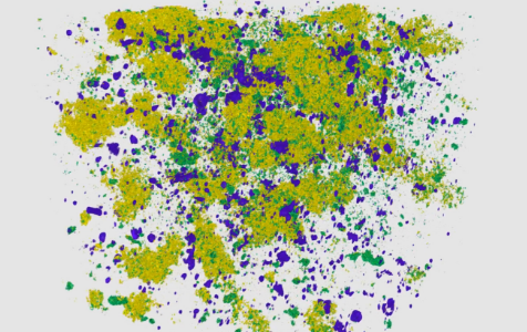
In the current opinion-rich media environment, providing contextual background to the data that underlies opinions is equally, if not more important, than providing the opinion itself. The same is true for microscopy, which tempts scientists and engineers to focus only on the tiniest details in the materials they investigate. But, suppose the cross section prepared by FIB is too small and made at a location without defects? Or 3D tomography is performed on a small volume at a shallow depth, revealing small grains overall? In both cases, the lack of context may lead to inaccurate conclusions.
Learn why visualizing complex details in your sample and using them in their full context is crucial for accurate conclusions!
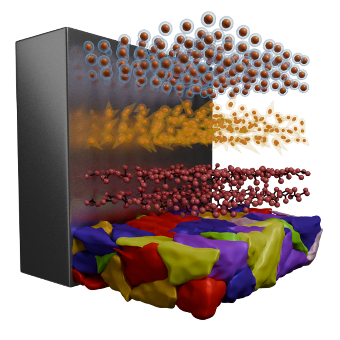
2D/3D UHR FIB-SEM characterization of materials
3D characterization with Xe Plasma FIB-SEM goes beyond the surface, revealing intricate structures with exceptional accuracy in three dimensions. This powerful combo of analytical techniques tackles larger volumes efficiently, reducing the risk of misleading results. Advanced analysis techniques like EDS / EBSD and ToF-SIMS unlock a wealth of elemental and structural details, enhancing the depth and accuracy of 3D analysis.

Obtain the best 3D characterization data from any sample


Detect light elements such as Li or C at ppm concentrations for Battery Research


Maximize sample characterization throughput for your 3D volume analysis

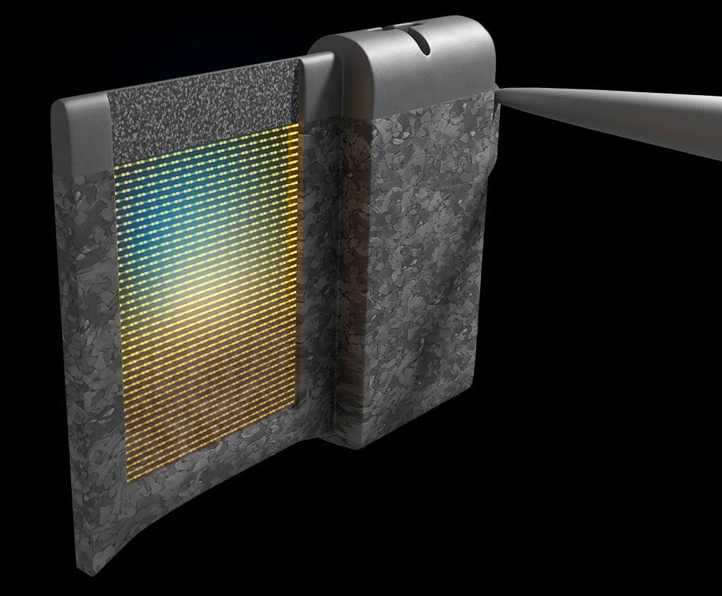
TEM sample preparation for STEM/TEM analysis
.png?width=476&height=300&name=MicrosoftTeams-image%20(34).png)
TEM preparation requires ultra-thin samples, often below 50 nm, for high-resolution imaging. Our FIB-SEM technology offers two configurations: the Gallium (Ga) Ion Beam, which is user-friendly and integrates well with existing TEM workflows, ideal for straightforward specimen preparations; and the Xenon (Xe) Plasma Beam, which provides greater versatility and produces specimens with minimal amorphization damage and the absence of ion implantation artefacts.

Prepare high-quality TEM specimens consistently, even without FIB-SEM expertise.


Achieve top-quality TEM specimens, even from highly demanding samples.


Minimize sample damage with gentle and precise final polishing.

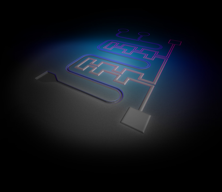
Nanoscale prototyping and nanofabrication
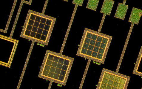
Nanoprototyping requires precise material manipulation to meet exact design criteria. Our FIB-SEM with a gallium (Ga) ion beam is ideal for this, offering precise cutting and deposition for nanoscale fabrication. It supports FIB-induced deposition (FIBID) and etching (FIBIE) for intricate nanostructures. The finely focused gallium ion beam excels in crafting detailed features without defects.

Prototype micro- and nano-devices like micropillars, cantilevers and microfluidic channels


Prepare nanofabricated structures from any material

Create three-dimensional nanopatterns like plasmonic half helix resonators
2D/3D UHR FIB-SEM characterization of materials
3D characterization with Xe Plasma FIB-SEM goes beyond the surface, revealing intricate structures with exceptional accuracy in three dimensions. This powerful combo of analytical techniques tackles larger volumes efficiently, reducing the risk of misleading results. Advanced analysis techniques like EDS / EBSD and ToF-SIMS unlock a wealth of elemental and structural details, enhancing the depth and accuracy of 3D analysis.
Obtain the best 3D characterization data from any sample
Detect light elements such as Li or C at ppm concentrations for Battery Research
Maximize sample characterization throughput for your 3D volume analysis
TEM sample preparation for STEM/TEM analysis
TEM preparation requires ultra-thin samples, often below 50 nm, for high-resolution imaging. Our FIB-SEM technology offers two configurations: the Gallium (Ga) Ion Beam, which is user-friendly and integrates well with existing TEM workflows, ideal for straightforward specimen preparations; and the Xenon (Xe) Plasma Beam, which provides greater versatility and produces specimens with minimal amorphization damage and the absence of ion implantation artefacts.
Prepare high-quality TEM specimens consistently, even without FIB-SEM expertise.
Achieve top-quality TEM specimens, even from highly demanding samples.
Minimize sample damage with gentle and precise final polishing.
Nanoscale prototyping and nanofabrication
Nanoprototyping requires precise material manipulation to meet exact design criteria. Our FIB-SEM with a gallium (Ga) ion beam is ideal for this, offering precise cutting and deposition for nanoscale fabrication. It supports FIB-induced deposition (FIBID) and etching (FIBIE) for intricate nanostructures. The finely focused gallium ion beam excels in crafting detailed features without defects.
Prototype micro- and nano-devices like micropillars, cantilevers and microfluidic channels
Prepare nanofabricated structures from any material
Create three-dimensional nanopatterns like plasmonic half helix resonators