TESCAN SOLARIS X,
a Plasma FIB-SEM
Powerhouse
Improve Package Level Failure Analysis with our Advanced Platform for Deep Sectioning and the Highest Resolution End-Pointing
Key benefits of TESCAN Plasma FIB-SEM
Purpose-Driven Performance
Accelerate efficient physical failure analysis with the rapid material removal capabilities of the Xe Plasma FIB beam.
Deep Sample
Access
Reach buried structures up to 1 mm in depth using a maximum ion beam current of 3 μA.
Precision at the Nanoscale
Achieve nanometer-precision end-pointing during milling or cross-sectioning with the high-resolution imaging of the Triglav™ SEM column.
Excellent surface sensitivity and high material contrast
Conduct ultra-high-resolution imaging on beam-sensitive materials using TESCAN's Triglav™ SEM column, designed for superb surface sensitivity and material contrast.
Pristine Sample Preservation
Prepare high-quality, damage-free TEM samples with the inert Xe ions of the Plasma FIB beam, eliminating Ga implantation or surface damage.
Artefact-free
results
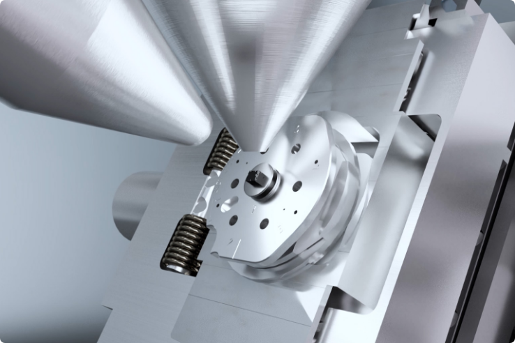
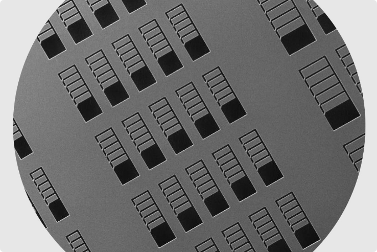
Create artefact-free cross sections, even on challenging composite materials, with our patented Rocking Stage for alternating milling angles and TRUE X-sectioning to utilize the most efficient center of the ion beam at highest currents.
User-Driven
Interface
Boost productivity for all users with advanced workflows in TESCAN's Essence™ graphical user interface.
Register for Our Webinar to Discover More about TESCAN Plasma FIB-SEM
TESCAN SOLARIS X for Semiconductor Packaging Failure Analysis
Dive deep into TESCAN Plasma FIB-SEM
Learn How to Prepare Extra-Large-Area Cross Sections in OLED Displays with TESCAN SOLARIS X
Unravel Complex Failures: Analyzing Next-Gen IC Packages & Devices
Perform Physical Failure Analysis of advanced stacked IC packages (2.5D, 3D IC), flip-chips, MEMS devices, OLED and TFT displays, MLCC capacitors, 3D NANDs, and many more.
Unveil Material Secrets: In-Depth 3D EDS & EBSD Microanalysis
Employ fast large-volume 3D EDS and 3D EBSD microanalysis of advanced packaging devices such as solder balls, TSVs, and bond pads for in-depth material composition analysis and characterization.
Uncover sub-surface features: Crafting Ga-Free TEM Lamellae for STEM Analysis
Produce precision, high-quality, Ga-free TEM lamellae under 100 nm in thickness from package and IC-level samples for subsequent STEM analysis.
Boost your analyses with our solutions
TESCAN Rocking Stage

Achieve Artifact-Free FIB Cross-Sectioning and Precise SEM End-Pointing for Challenging Samples.
TESCAN True X-Sectioning

Save time with ripple-free plasma FIB cross-sectioning that doesn't compromise high beam current.
Questions?
Interested in a virtual demo?
Our global team is ready to answer questions about TESCAN FIB-SEMs and our solutions for Semiconductors and IC Packaging Failure Analysis.

