Webinar Announcement: New insights from Semiconductor Failure Analysis with TESCAN's Integrated Workflow

A Comprehensive Approach to Semiconductor FA 

Do you wish to stay abreast of the ever-evolving landscape of semiconductor technology and its impact on device efficiency and reliability? Join us on January 23rd, 2024, for a captivating webinar that will expand your perspective on semiconductor failure analysis.  

Guided by Lukas Hladik, Product Marketing Manager at TESCAN Group, this online session promises to bring new insights for professionals in the semiconductor industry. 


Webinar Title: “Streamlining Millimeter-Scale Semiconductor Failure Analysis: An Integrated Workflow with Plasma FIB-SEM, Laser Techniques, and Advanced FA Tools”

Date and Time: January 23rd, 2024, from 9 A.M. and 5 P.M.


A Comprehensive Approach to Semiconductor FA 


Do you wish to stay abreast of the ever-evolving landscape of semiconductor technology and its impact on device efficiency and reliability? Join us on January 23rd, 2024, for a captivating webinar that will expand your perspective on semiconductor failure analysis. 


Guided by Lukas Hladik, Product Marketing Manager at TESCAN Group, this online session promises to bring new insights for professionals in the semiconductor industry. 


Webinar Title: “Streamlining Millimeter-Scale Semiconductor Failure Analysis: An Integrated Workflow with Plasma FIB-SEM, Laser Techniques, and Advanced FA Tools” 

What to Anticipate: 

  • Navigating the Miniaturization Maze: Discover how advancements in miniaturization, component integration, and optimization are transforming the performance and power consumption of electronic devices, including displays and batteries. 
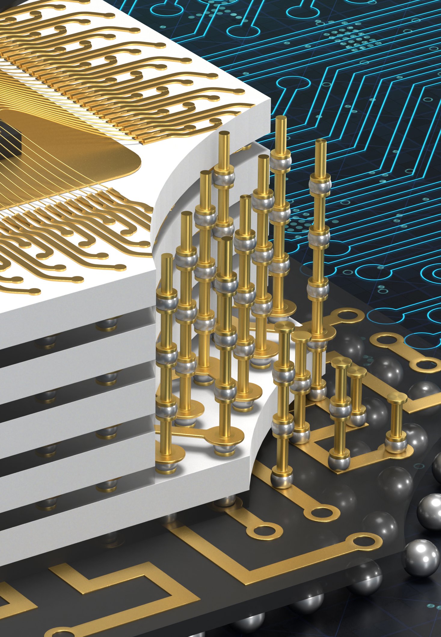
  • The Imperative of Rapid Failure Analysis: Learn about the escalating challenges in detecting defects beneath complex surfaces and the critical role of swift and accurate failure analysis in accelerating market readiness and ensuring device dependability. 
  • Innovations in Workflow Integration: Explore the dynamic integration of plasma FIB technology with high-speed laser ablation techniques (3D-Micromac microPREP™ PRO), enhancing the speed and precision of semiconductor failure analysis. 
  • Introducing TESCAN’s Large Volume Workflow Update: Delve into the latest enhancements, developed in collaboration with the European FA4.0 project, including a versatile shared sample holder and the pioneering Essence AutoSection™ software for automated alignment and ROI identification. 


What You Will Gain  

Participants will be treated to practical demonstrations on a variety of challenging samples, showcasing the workflow’s adaptability in handling complex devices and non-conductive materials.  

Together, we will learn how these state-of-the-art techniques enable rapid, artifact-free sample preparation, essential for ultra-high-resolution SEM imaging and comprehensive failure root-cause analysis. 

TESCAN-Semiconductors-failure-Analyses-banner-1080x1080px-02-webinar-in

Reserve your spot now and join a community of experts at the forefront of semiconductor technology advancements.


Meet the Expert

Lukas Hladik, a seasoned Product Marketing Manager at TESCAN Group, has been instrumental in the company since 2012. With a focus on Plasma FIB-SEM and failure analysis solutions, his expertise is deeply rooted in semiconductor R&D and closely aligned with the global semiconductor industry.