Webinar Highlights:
- Introduction to IC Delayering Challenges: Understand the complexities of semiconductor scaling down to sub-14 nm technology nodes and its implications for failure analysis and quality control.
- Advanced Delayering Techniques: Explore the new advancements by TESCAN that include Low Angle Polishing and “drilled nozzle” technologies, which allow for uniform removal of metal layers and large delayered areas of up to 300x300 µm².
- Real-World Applications: Gain insights into actual delayering processes of 7 nm and 5 nm devices, starting from metal 14 down to the transistor contact layer, all within one advanced instrument.
- Automated End-Pointing Capabilities: Learn about the automated processes that facilitate precise end-point detection on selected layers during the delayering process.
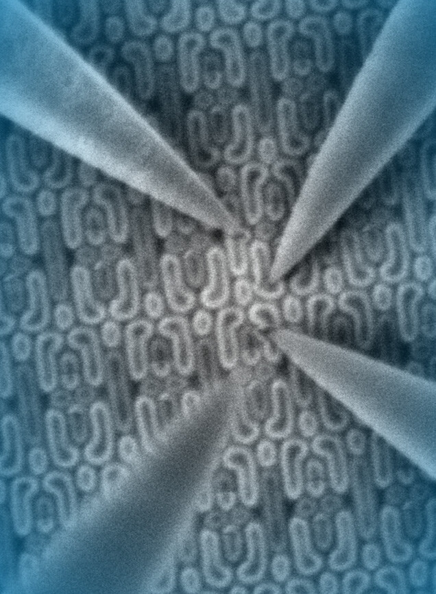
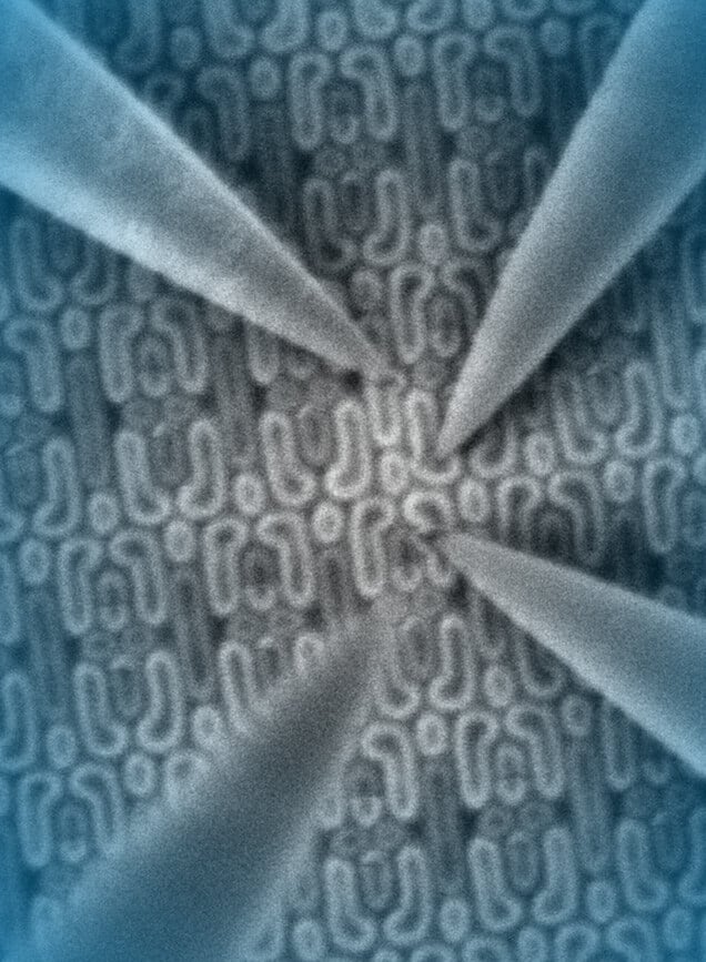
- Complete Nanoprobing Workflow: Experience the integration of Imina Technologies’ nanoprobing platform with four miBots™, demonstrating the seamless workflow within TESCAN’s CLARA instrument for enhanced electrical analysis.
Interactive Expert Guidance
Get your questions answered by industry leaders with deep insights into the practical challenges of nanoscale device analysis
Leading through the session are Lukas Hladik from TESCAN, a renowed expert in FIB-SEM technologies, and Guillaume Boetsch, co-founder of Imina Technologies, both bringing years of expertise in precision robotics for microscopy.
We are excited to offer this detailed look into the future of semiconductor device analysis, featuring real-world applications and technological advancements. Join us and be part of shaping the future of nanotechnology!
Registration was closed