The authors address the challenges associated with accessing deeply buried structures in microelectronic devices for physical failure analysis (PFA). Traditional methods, like mechanical polishing or Ga+ FIB milling, are either too slow or too damaging for large-volume sample preparation. The paper proposes a method that combines the fast material removal rates of a ps-laser ablation tool with the precise end-pointing and fine surface polishing capabilities of a Xe Plasma FIB-SEM system. The paper proposes that this method enables quick and accurate PFA of microelectronic devices, as well as increased productivity due to the simultaneous and continuous operation of both tools.
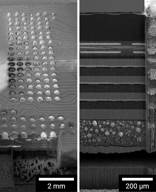
 The research demonstrates the effectiveness of the proposed method on various applications, such as preparing damage-free and delamination-free cross-sections of an AMOLED mobile display, which is composed of sensitive materials and complex structures. Preparing cross-sections of flip-chip packages with different solder ball materials and sizes, which require high-resolution imaging and analysis, is also discussed in this paper, as well as CAD navigation, data correlation, and bitmap overlays for end-pointing. CAD navigation, data correlation, and bitmap overlays for end-pointing.
The paper also covers related issues, such as CAD navigation, data correlation, and bitmap overlays for end-pointing. The paper shows that the proposed method can produce high-quality cross-sections with minimal artefacts and damage, and can reveal defects such as cracks, voids, intermetallic compounds, and delamination.
Optimise your Semiconductor Failure Analysis with TESCAN Solutions: Master IC Packaging Failure Analysis with TESCAN Solutions
Learn about this compelling research: Pairing Laser Ablation and Xe Plasma FIB-SEM: An Approach for Precise End-Pointing in Large-Scale Physical Failure Analysis in the Semiconductor Industry | ISTFA Proceedings | ASM Digital Library (asminternational.org)
Optimise your Semiconductor Failure Analysis with TESCAN Solutions: Master IC Packaging Failure Analysis with TESCAN Solutions