DOWNLOAD
Delayering sub-20 nm nodes for in-situ nanoprobing with TESCAN AMBER X
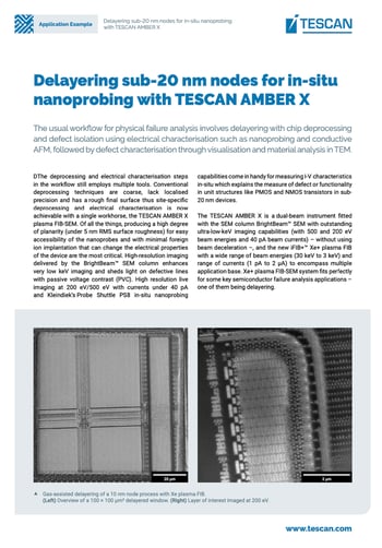
The usual workflow for physical failure analysis involves delayering with chip deprocessing and defect isolation using electrical characterisation such as nanoprobing and conductive AFM, followed by defect characterisation through visualisation and material analysis in TEM.