How AMBER 2 Empowers Your Research
TESCAN AMBER 2 is a fully automated Ga FIB-SEM for routine TEM sample preparation, nanoscale characterization, and prototyping.
Offering precision and ease of use, it delivers exceptionally high FIB image quality even at low accelerating voltages. The field-free BrightBeam™ SEM column ensures high contrast nanoscale imaging and exceptional sample versatility.
Whether preparing TEM samples, creating nanostructures, or characterizing nanomaterials, AMBER 2 is the perfect tool for a variety of use cases.


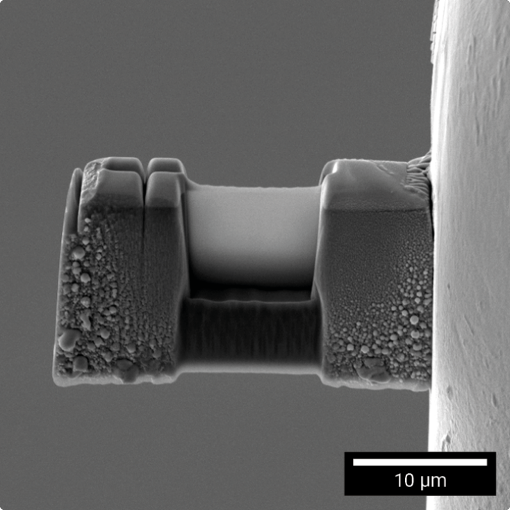
Image showing TEM specimen prepared automatically in less than 1h using TEM AutoPrep ProTM
Automated TEM Preparation

Prepare high-quality TEM samples automatically with minimal damage.
Advanced TEM Lamella Preparation

Achieve excellent quality, optimal geometry and minimal amorphization damage in TEM samples.
FIB
Nanoprototyping

Fabricate, create or modify materials into functional devices using a single FIB-SEM instrument.
Advanced SEM
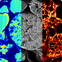
Contrast Methods

Enhance surface sensitivity and detect different phases more effectively.
Electron Beam Lithography

Craft precise functional prototypes at nano and micro scales with TESCAN own Electron Beam Lithography and Fast Beam Blanker.
User-friendly

Obtain high-quality data without needing extensive FIB-SEM expertise
Watch our TESCAN AMBER 2
webinar
Key benefits of AMBER 2
Automate your TEM sample preparation workflow with TESCAN AMBER 2, a field-free Ga FIB-SEM system offering an easy, dependable solution for automated and versatile TEM specimen preparation.
Explore new TEM possibilities
by preparing inverted or planar samples and transferring them to the grid with a nanomanipulator for precise feature orientation.
%20kopie.png?width=214&height=214&name=MicrosoftTeams-image%20(46)%20kopie.png)
Fabricate, create, or modify functional devices with AMBER 2’s capabilities for electron beam lithography, ion beam prototyping, FEBID, or FIBID, enhancing design flexibility and creativity.
.png?width=214&height=214&name=MicrosoftTeams-image%20(29).png)
Simplify FIB-SEM operation with TESCAN Essence™ software, automating SEM and FIB alignments and providing advanced stage collision protection for all skill levels.
Perform ultra-high-resolution imaging and nanoanalysis
on diverse materials with the BrightBeam™ field-free UHR-SEM column and high current Orage™ FIB column, ensuring excellent performance and versatility.
Gain deeper material insights with AMBER’s multimodal detection system, enabling simultaneous acquisition of multiple signals.