
Experience the power of nanoscale fabrication and rapidly create functional device prototypes with TESCAN's cutting-edge FIB-SEM technology. Our smart and efficient system is designed to make nanoprototyping accessible and cost-effective for laboratories of all kinds, from microelectronics to automotive and scientific equipment industries.
Don't let your ideas stay on paper. Turn them into reality with TESCAN's advanced nanoscale prototyping and fabrication solutions.

Nanoscale Prototyping of Functional Devices Using FIB Milling and the Widest Selection of Proprietary Gas Precursors

Essence™ DrawBeam
expandable software module for high precision nanopatterning and nanofabrication applications
Essence™ DrawBeam is a modular, fully integrated patterning engine for FIB-SEM applications such as cross-sectioning, sample preparation for TEM, atom probe tomography, or mechanical testing. DrawBeam handles advanced operations like patterning and creating complex structures using focused electron beam-induced deposition (FEBID), focused ion beam induced deposition (FIBID), and other user-defined focused ion beam (FIB) milling processes.

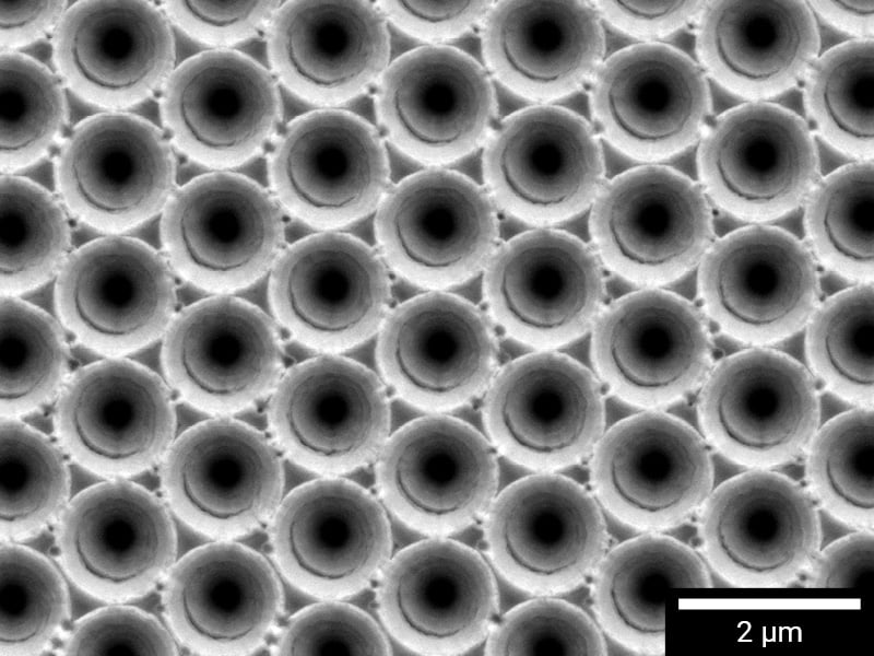
Prototype micro- and nano-devices like micropillars, cantilevers and microfluidic channels
Micro and nanoscale prototyping of structures requires clear definition of their shapes and milling strategies. Whether as a newcomer or an advanced user in nano prototyping, you’ll benefit from a rich library of purpose-designed nano prototyping objects dedicated to the preparation of complex nanostructures.
Prepare nanofabricated structures from any material
Devices and structures can be milled into (or deposited on) a wide range of materials. Define various FIB-related parameters using advanced features, such as editable multi-material databases in EssenceTM DrawBeam, to achieve maximum milling depth or deposition height precision on almost any substrate material.
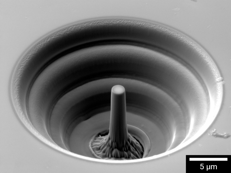
Produce artifact-free repetitive nanostructures
The final quality of the structures depends on the strategy of handling intersections of overlaying objects and the order of the objects in the project. Choose between serial or parallel object patterning with the option to merge overlapping objects, resulting in the highest quality of nanostructures.
TESCAN FIB-SEM Expert PI & VisualCoder
An intuitive software interface for workflow development and automation—accessible to both programmers and non-programmers.
This powerful tool streamlines repetitive tasks, enhances efficiency, and enables the development of advanced SEM and FIB imaging and milling strategies for rapid prototyping, all within the TESCAN Nanoprototyping Toolbox. Designed to meet the needs of researchers and technicians, it offers a flexible dual-scripting environment:
Expert PI provides an extensive library of SEM/FIB-SEM scripting tools for precise control and customization.
VisualCoder delivers a user-friendly, block-based interface for effortless, no-code programming.
Whether you're optimizing imaging workflows or automating complex processes, TESCAN FIB-SEM Expert PI & VisualCoder empower you with the tools to push the boundaries of nanoprototyping.

Improve overall quality and assure perpendicularity of FIB nanofabricated structures such as cantilevers
Make use of the patented TESCAN Rocking Stage and correct the taper angle for any material in both X and Y direction. This is especially powerful when preparing samples for synchrotron or cantilever samples for in-situ mechanical testing at the nanoscale.

TESCAN Rocking Stage
TESCAN Rocking Stage is fully compatible with TESCAN nano-fabrications workflows. As such, it enables an additional tilt axis to mitigate geometrical asymmetries caused by tempering the angle.

Nanoscale Prototyping of Functional Devices Using Electron Beam Lithography
Perform electron beam lithography by combining advanced EBL software and TESCAN’s fast electrostatic beam blanker
Whether you're a seasoned expert or new to EBL, TESCAN's advanced Fast Beam Blanker provides the perfect solution for achieving creative freedom in your work.
Work confidently with the full support of the GDSII hierarchical data format
Define and modify intended EBL steps and workflows for multi technique exposure with ease through an add-on for the third party open source software Klayout.
Tailor your EBL exposure strategy
Field stitches can be a major obstacle when it comes to achieving the desired exposure quality in EBL designs. That's why TESCAN offers a solution that puts manual control over field placement in your hands. By avoiding stitching errors, you can achieve the optimum final exposure quality for your work.
Optimize exposure conditions
Continual beam current control and theoretical beam spot size estimation enable users to match the exposure step size to the probe diameter. This means the smoothest possible sidewall for the exposed structure is achieved.
Plan your time requirement for instrument use
Maximize your instrument's usage with the exposure time estimate feature. This feature enables offline exposure simulation to allow optimization and debugging of the exposure parameters, resulting in a more robust design and shorter writing times when actually prepared on the instrument.

E-beam lithography
TESCAN’s EssenceTM EBL Kit works with TESCAN’s fast electrostatic beam blanker to provide a fully integrated solution for performing EBL using a FIB-SEM. This provides the flexibility not only for routine imaging and analysis but also for nanofabrication. The EssenceTM EBL kit, coupled with the powerful FIB nanofabrication engine of a FIB-SEM, creates a powerful tool for rapid prototyping of functional devices in fundamental and applied research of materials.
