
Plasma FIB-SEM, Redefined
TESCAN AMBER X 2 combines pristine FIB resolution, excellent ion beam parameters and a field-free SEM column to redefine speed, accuracy and utility in sample preparation and characterization.
Meet AMBER X 2, Our Most Advanced Plasma FIB-SEM
When it comes to plasma FIB-SEM, TESCAN AMBER X 2 is as state-of-the-art as it gets. A holistic solution for materials science research, it prepares high-quality TEM samples, analyzes the structure and chemistry of materials in both 2D and 3D, and provides correlative multimodal analytical information with unmatched speed and precision.
With its unique field-free SEM column and the latest Mistral™ Plasma FIB column, AMBER X 2 stands out as the most adaptable, flexible, and user-friendly plasma FIB-SEM on the market.


How TESCAN AMBER X 2 Empowers Your Research
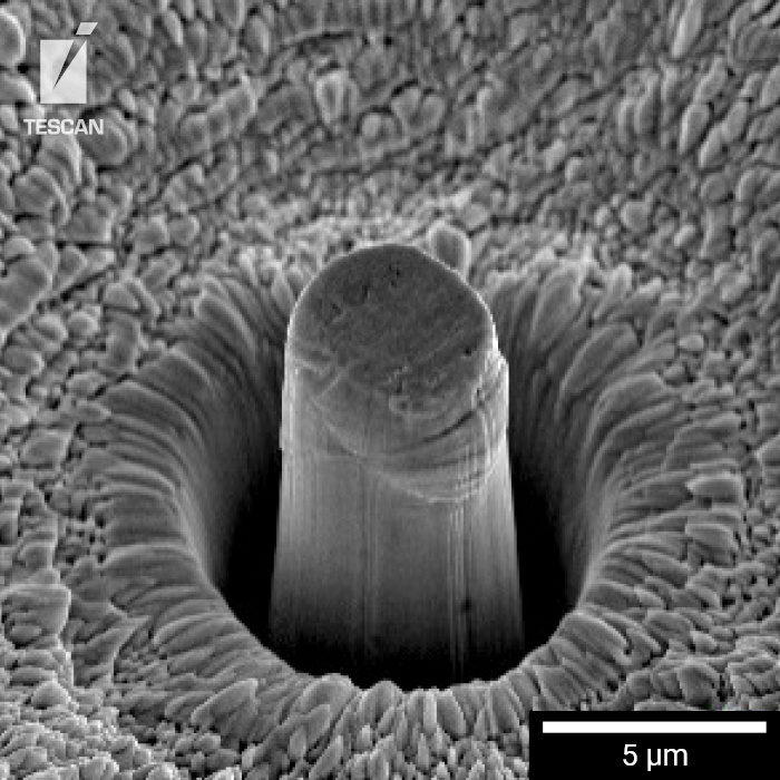
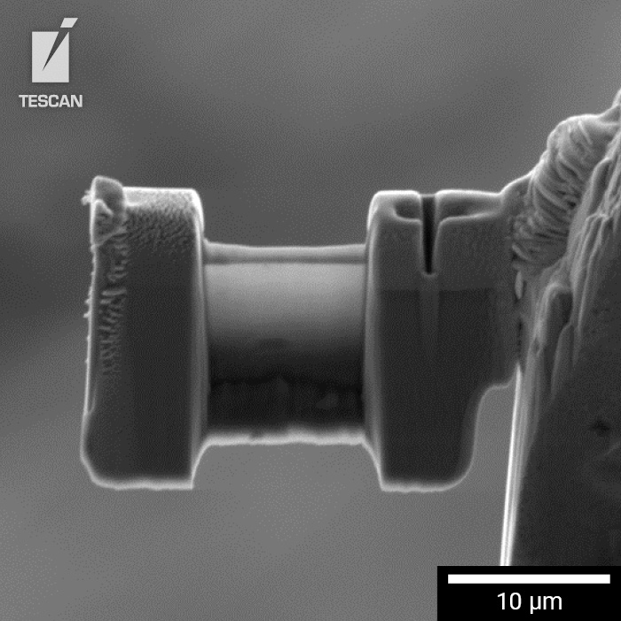
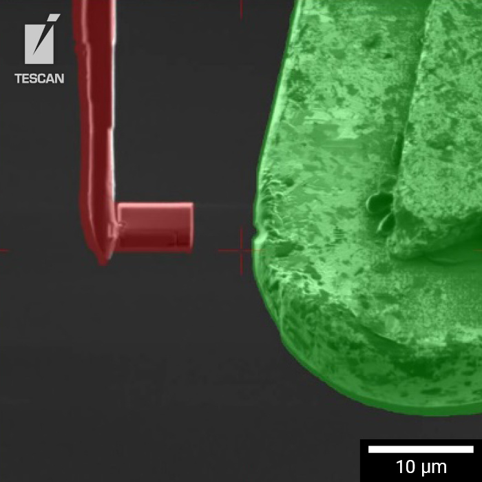
Automated TEM Lamella Preparation

FIB-SEM Analysis, Fast and Precise

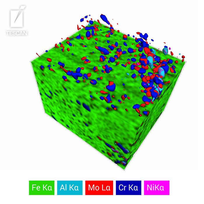
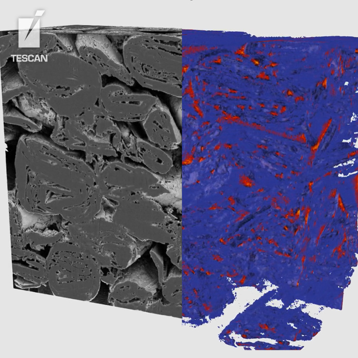
Novel 3D Multimodal Insights

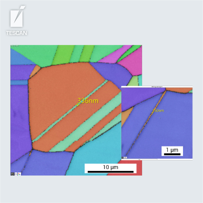
Advanced Contrast Methods

User-friendliness

Sample Compatibility Excellence

A New Dimension of Material Understanding
TESCAN AMBER X 2 goes beyond traditional analysis, offering a gateway to a whole new world of 3D insights into the morphology, composition, crystallography, and chemistry of your samples. Combine the power of EDS, EBSD, and ToF-SIMS data to reveal the hidden secrets of your materials in stunning 3D detail.
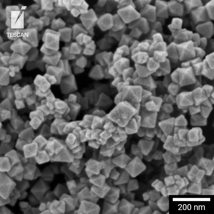
Unprecented Detail. Unlimited Exploration.
TESCAN AMBER X 2 allows you to delve deeper into the heart of your materials than ever before. Explore the finest details and uncover previously unseen features and contrasts across a vast range of materials, encompassing metals, ceramics, polymers, and even biomaterials. Field-free BrightBeam™ Technology with Energy Filtering allows you to image your samples with exceptional clarity and minimal damage, utilizing low landing energies for optimal results.
This combination empowers you to push the boundaries of your research and make new discoveries in a variety of fields.


